Authored by Ruben Medina
E-mail: medina72@unlv.nevada.edu
Date: 11/22/13
In order to have an 8-bit ALU the components used in the schematic design were the 8x parallel components created in lab 7.
After creating a new project library to hold the ALU, I used the cross-library copy function to copy over the 8-bit AND, 8-bit OR, 8-bit full-adder (including layout), 8-bit inverter and 2-to-1 mux from lab 7.
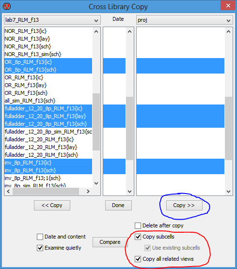
Note the selection of copy subcells and copy all related views options to make sure all associated parts for the copied components are also copied into the new library.
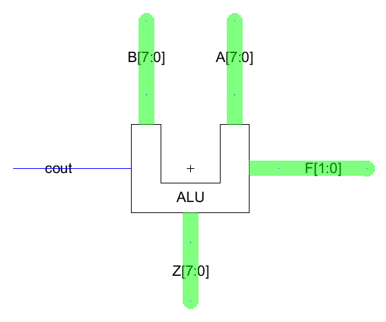
The ALU will implement the AND, OR, Addition, and Subtraction functions for the 8-bit A and B input buses and the result will be output to the 8-bit Z bus.
The functions will be selected by the 2-bit F input bus as can be seen in the table below:
|
F[1:0] |
Function |
| 00 | AND |
| 01 | ADD |
| 10 | OR |
| 11 | SUB |
The schematic and icon for the ALU were drafted as follows:
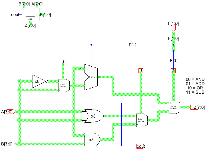
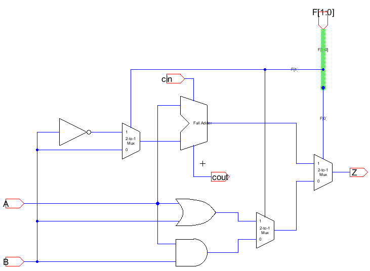
The subtract function is implemented by inverting the B input of the full-adder and setting the carry in of the full-adder to 1 for two's complement. This is done by using the F[1] bit as an input to a 2-to-1 mux to select the inverted B input bus and also set the carry in bit of the full-adder.
The AND and OR functions are easily added by placing the 8-bit AND and OR components and three 2-to-1 muxes are used to select the desired function using the F bus.
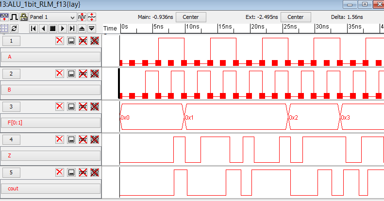
To simulate the ALU, I created a separate simulation schematic using the ALU icon previously created.
I then created an IRSIM command file containing vectors for all of the inputs and outputs which is located here and simulated the ALU.
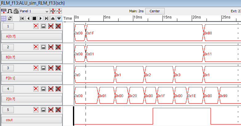
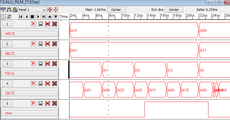
In my simulation commands I set the output bus to 0 for 2ns after selecting the function before setting the output bus to tri-state("x") to show the result because otherwise the Z output bus is squeezed together and hard to read in the simulation as the final output is calculated for the addition and subtraction functions as can be seen below:
We can see from the simulation that the first function simulated is AND (00) and the result 0x1F AND 0x01 = 0x01 is correct.
Next, the function simulated is the addition operation (01) and the result 0x1F + 0x01 = 0x20 is correct.
Next, the function simulated is OR (10) and the result 0x1F OR 0x01 = 0x1F is correct. (With one note, see below)
Next, the function simulated is subtraction (11) and the result 0x1F - 0x01 = 0x1E with a carry-out of 1 which is correct.
Finally, the input buses A and B are changed to 0x88 and 0x11, respectively, and the addition function is set for the result 0x88 + 0x11 = 0x99 which is correct.
Note: The cout bit is set high during the OR function operation. This is due to the fact that the F[1] bit of the OR function is also used to select the inverted B input bus and set the carry-in of the full-adder for the subtraction operation. Thus, this output should be disregarded during the operation of the OR function. One way to correct this would be to add an AND gate with the F[1:0] bits as input so this only happens for subtraction (11) but this introduces an additional gate delay during simulation.
My jelib of the project containing the schematic and icon can be found here.
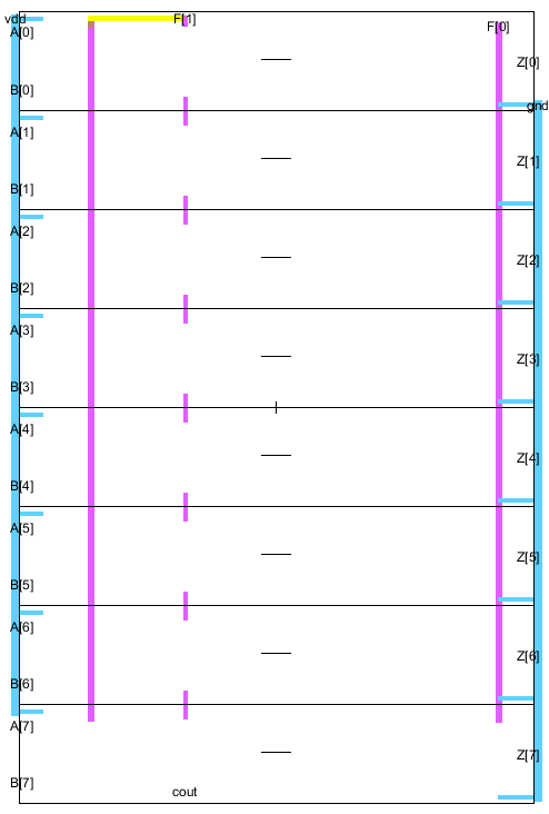
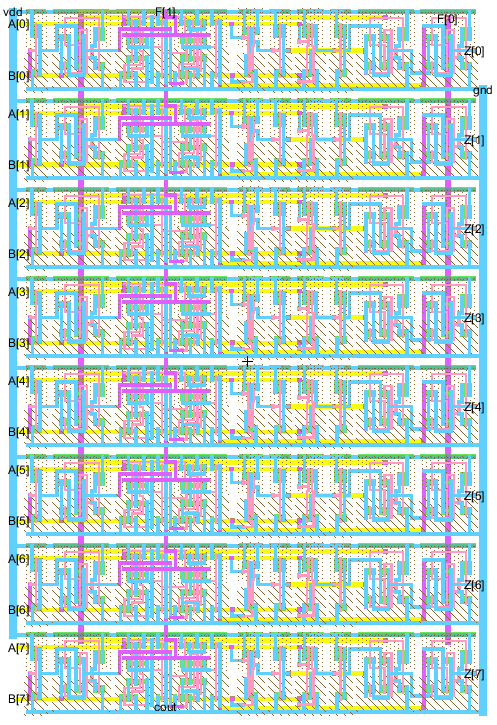
To complete the layout of the complete 8-bit ALU I decided to split the layout into separate 1-bit ALU components. This saves time by only needing to layout 1-bit and also leads to a clean and compact layout for the 8-bit ALU.
To accomplish this, I began by making a new schematic containing only 1-bit components of the previous 8-bit ALU schematic.
Next, I did the layout for this 1-bit ALU.
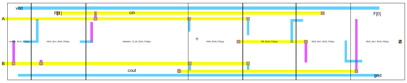
And opened:
And the 3D view:
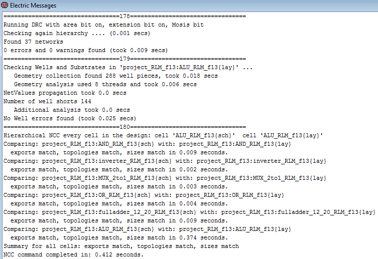
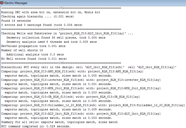
Next, I ran DRC, well, and LVS checks on the layout:
I then simulated the schematic and layout to make sure this new 1-bit ALU was working correctly using the IRSIM command file here:
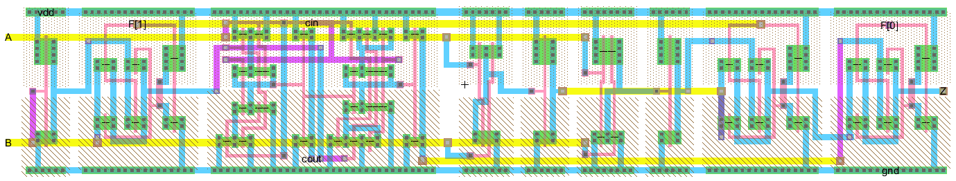
With the 1-bit ALU layout completed, I began the layout for the 8-bit ALU.
To layout the 8-bit ALU I used 8 of the 1-bit ALU layouts stacked on top of each other and then made the appropriate connections to match the schematic. This included connecting all of the F[0] inputs together and all of the F[1] inputs together while also connecting the first ALU bit's cin input to F[1] and all of the couts and cins for each bit together. I also connected the vdd and ground for all of the bits together and made the necessary exports of vdd, gnd, F[1:0], A[7:0], B[7:0], Z[7:0], and the last bit's cout.
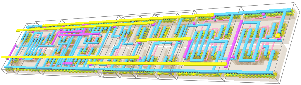
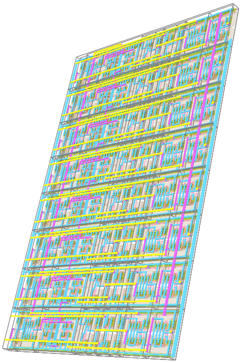
The 3D view can be seen below:
Next, I ran DRC, well, and LVS checks which can be seen below:
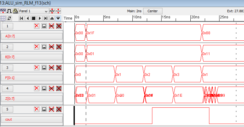
Finally, I re-simulated just the layout of the 8-bit ALU which results in the same simulation as the schematic but with the result of the addition of 0x88 and 0x11 taking slightly longer to stabilize:
My jelib of the project containing the schematic, icon, and layout can be found here.
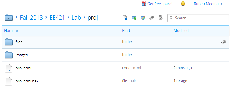
To make sure nothing was lost I backed up my project folder containing the project library and this webpage to Dropbox: