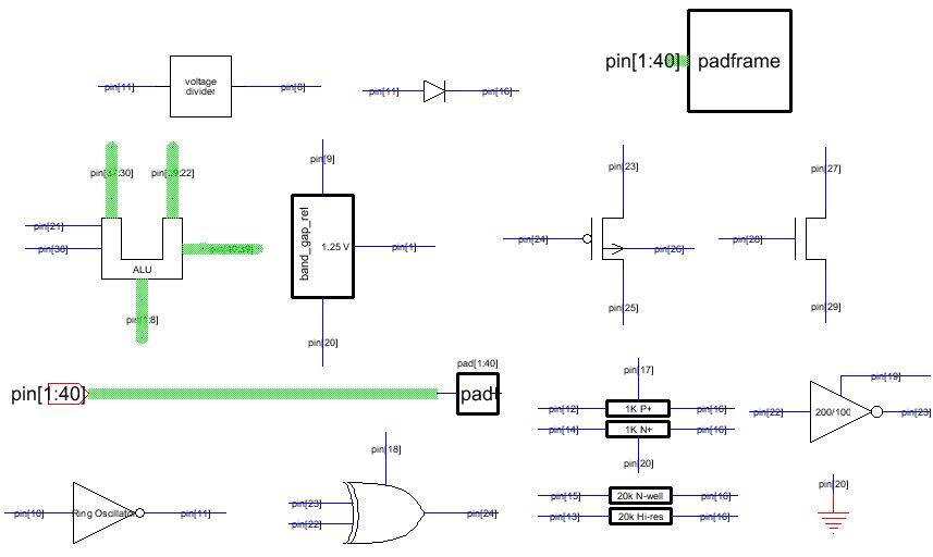
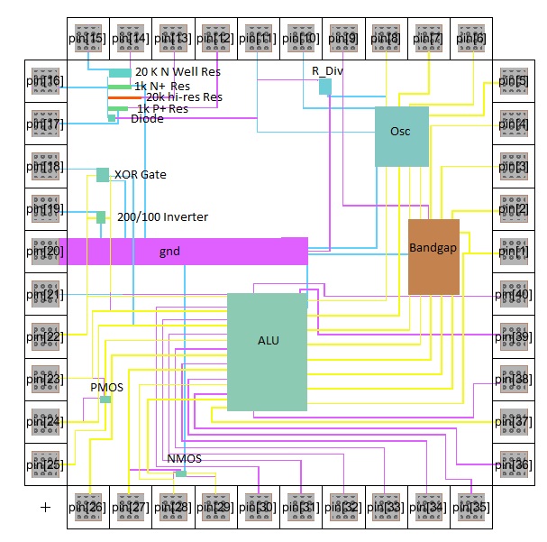
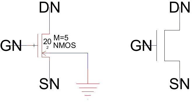
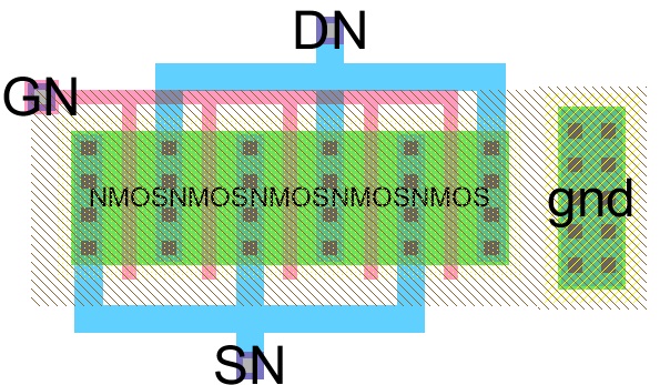
100/2 NMOS with 3 pins (DN, GN, SN)
Schematic of 100/2 NMOS
Layout of 100/2 NMOS
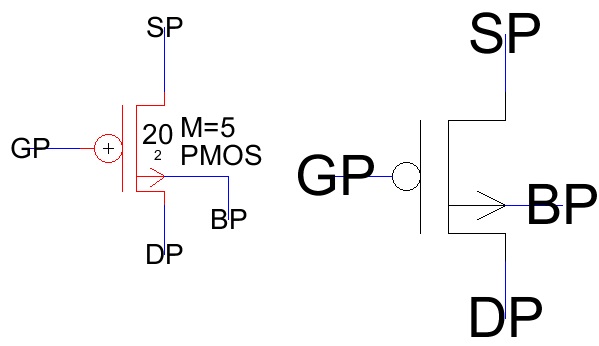
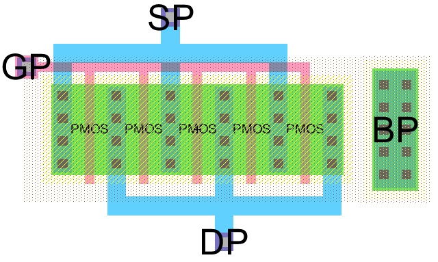
100/2 PMOS with 4 pins (DP, GP, SP, and BP)
Schematic of 100/2 PMOS
Layout of 100/2 PMOS
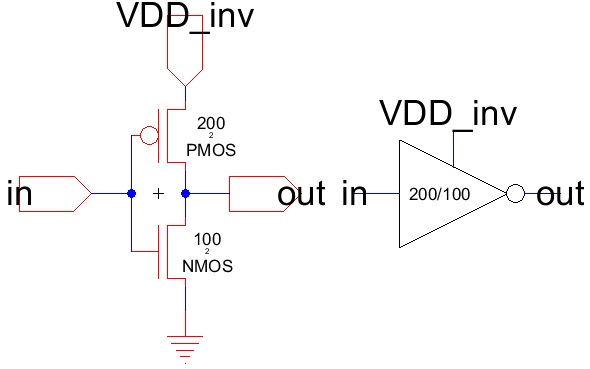
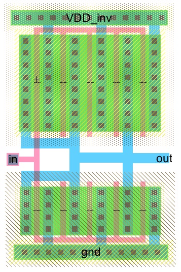
Inverter made using 100/2 NMOS and 200/2 PMOS with 3 pins (in, out, VDD_inv)
Schematic of Inverter
Layout of Inverter
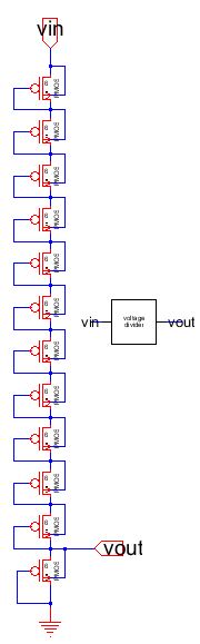
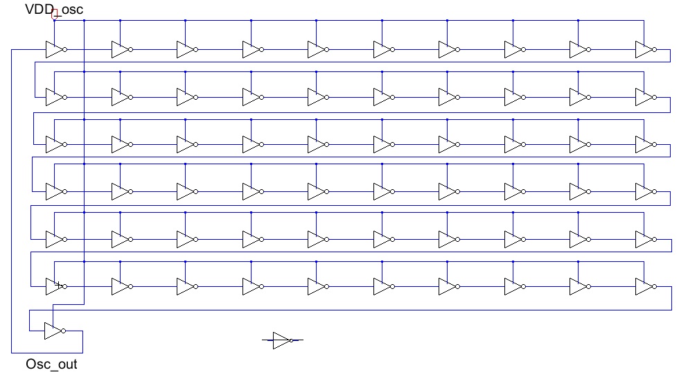
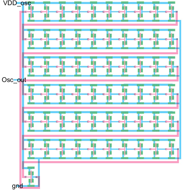
61 stage ring oscillator using 10/2 MOSFETS with off-chip buffer and 2 pins (VDD_osc and Osc_out)
Schematic of ring oscillator
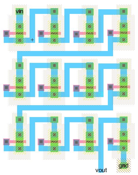
Layout of ring oscillator
20k n-well resistor with 2 pins
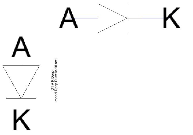
Schematic of 20k n well resistor

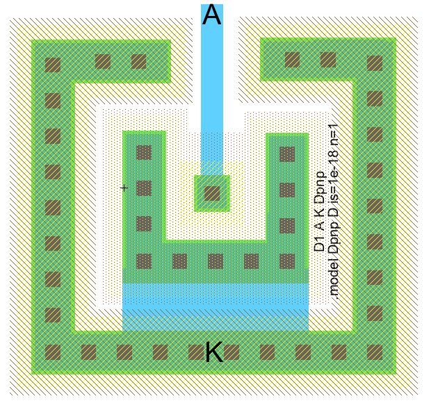
Layout of 20k n well resistor
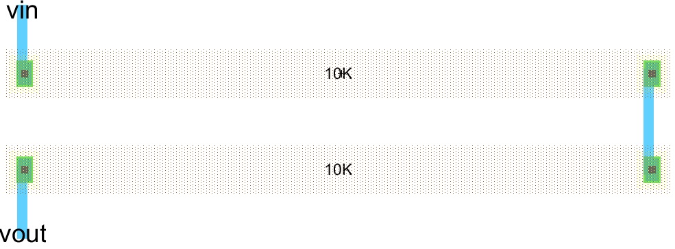
20k hi-res poly resistor
Schematic of hi-res poly resistor

Layout of hi-res poly resistor

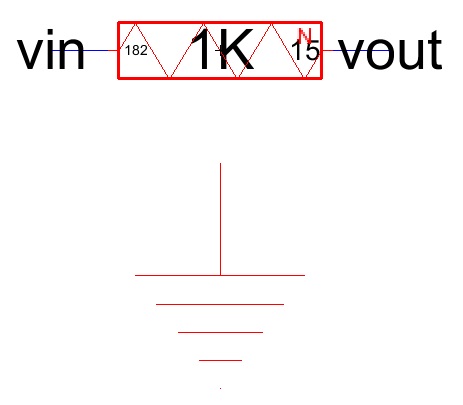
1k n+ resistor
Schematic of 1k n+ resistor
Layout of 1k n+ resistor

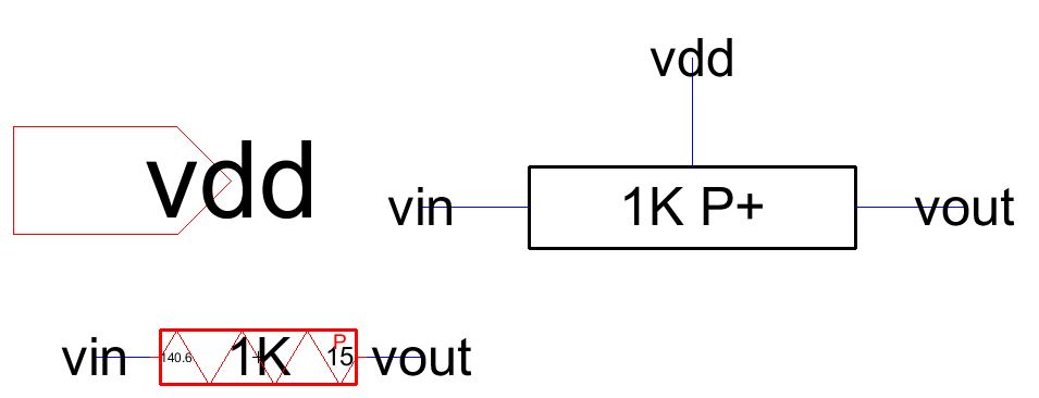
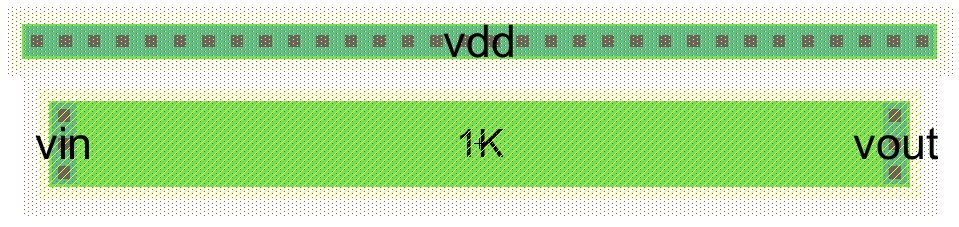
1k p+ resistor
Schematic of 1k p+ resistor
Layout of 1k p+ resistor
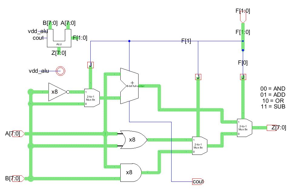
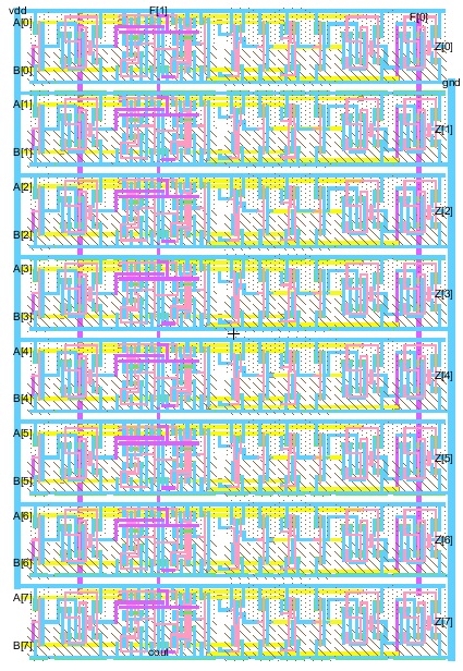
8 bit ALU with 28 pins (8 pins for A[0:7], 8 pins for B[0:7], 8 pins for Z[0:7], 2 pins for F[0:1], and VDD)
Schematic of 8 bit ALU
Layout of 8 bit ALU
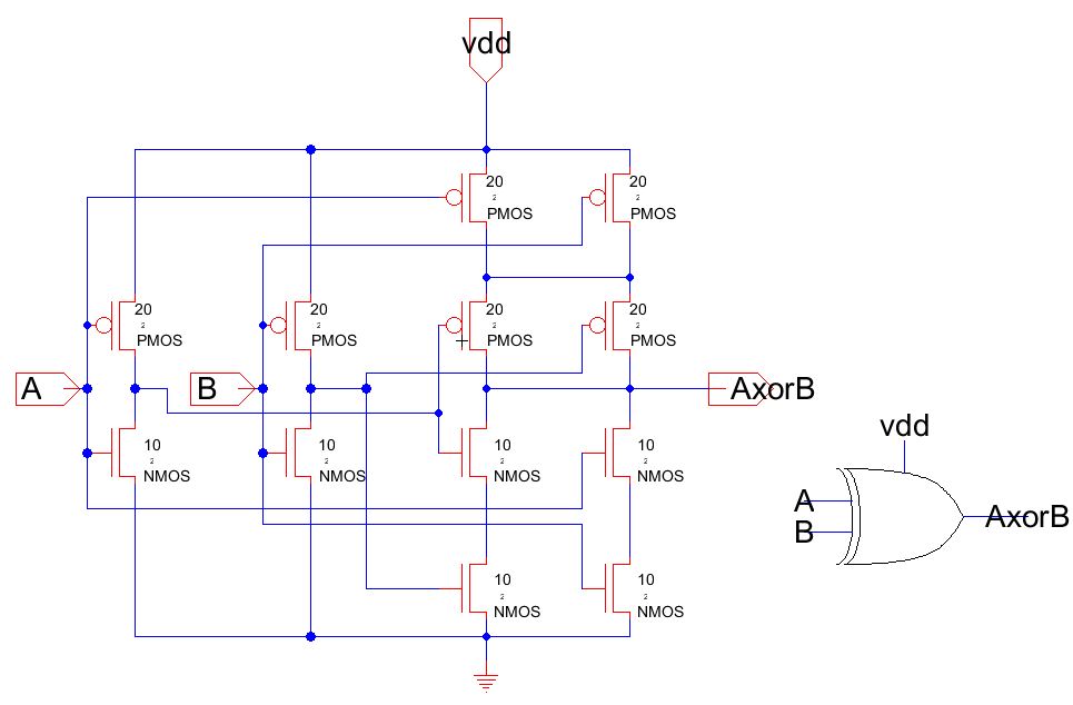
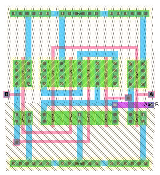
XOR Gate with 3 pins (A, B, VDD)
Schematic of XOR gate