Lab 6 -
ECE 421L
Authored
by Stryder Loveday
loveday3@unlv.nevada.edu
October 11, 2013
In this lab, we will be
creating the Schematic and Layout of a NAND, NOR and XOR gate, then
combine them for form a Full Adder. Tutorial 4 and Electric video
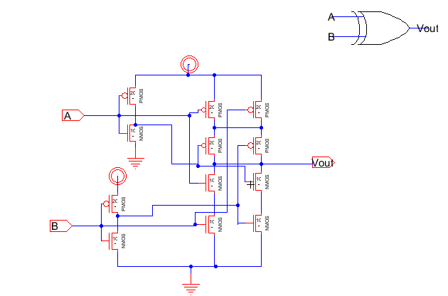
11 should be reviewed prior to this lab. The NAND uses 10/2 for
NMOS and PMOS, while the NOR and XOR uses 10/2 for NMOS and 20/2 for
PMOS.
First, a schematic for a NAND gate will be built, and a layout will be created.

Once
the circuit has been created, create an icon view, using a standard
NAND symbol as seen below. The circuit will now be tested with
Spice and IRSIM.
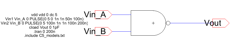

As

As
can be seen, the NAND behaves as it should, with the output only
becoming 0 when both inputs are 1, after the settling time. Now,
a NOR gate will be constructed.

Again, create an icon view with appropriate shape. The NOR will now be tested.


The
NOR operates as it should, with the output becoming 0 unless both
inputs are 0. Now, an XOR will be constructed. Note that an
XOR requires the use of two inverters, to create complimentary inputs.


As
can be seen, the XOR works as an OR gate, with either of the inputs
being able to bring the output high, while if both outputs are
simultaneously high, the output will be 0. Now, the gates will be
combined to forma Full Adder circuit.


The
results show that the Full Adder behaves as expected. If one of
the inputs is high, S goes high. If two inputs are high, Cout
goes high. If all three inputs are high, both S and Cin go high.
Now, the gates and full adder will have layouts created.
Remember to well check and to follow all design rules.
NAND:

NOR:

XOR:

The Full Adder combines the NAND and XOR gates to be created.

A
link to my .jelib file is located here.
This
concludes the Lab 6 report for EE 421. Please direct
any comments or suggestions to Stryder Loveday, at the e-mail address
listed above.
Return
to EE 421L Labs