Lab 2 - ECE 421L
In this lab we will be designing a basic DAC using N-well resistors. The DAC is constructed with a combination of R and 2R resistors.
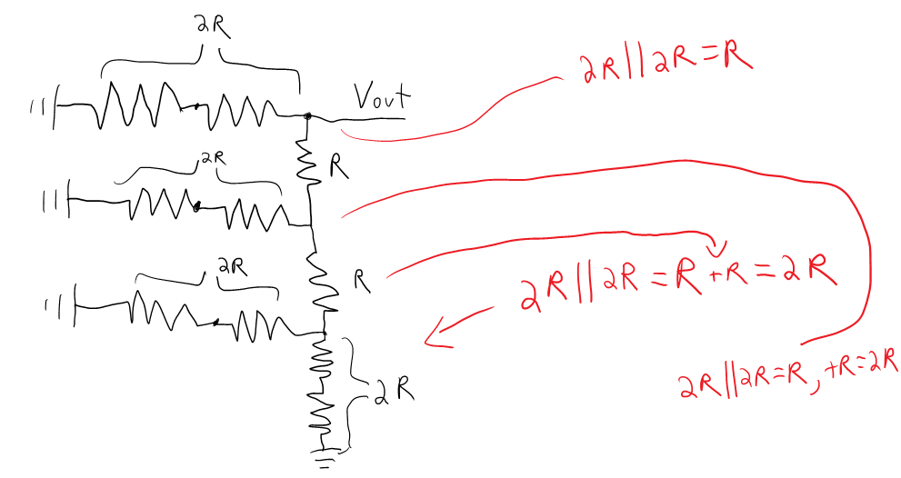
To determine the output resistance of the DAC, we can Thevenize the circuit, and the output resistance is determined to simply be R.
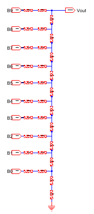
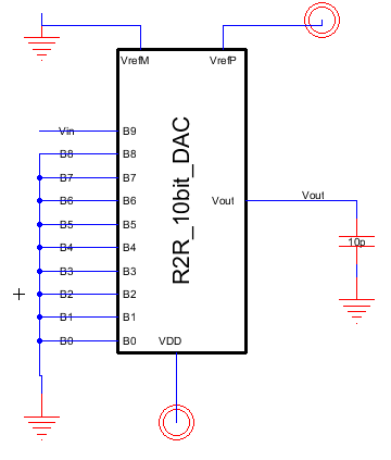
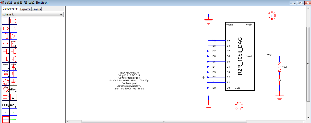
The finished DAC construction is of a 10-bit DAC, constructed similarly to the example above.
By cascading the R-2R pairs, we can extend this DAC to as many bits as needed.
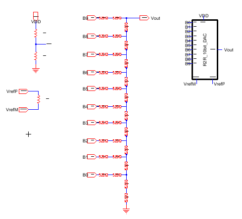
Next, we need to include some support circuitry and create an icon to represent our circuit so we can use it in other schematics. To create an icon, go to View -> Create Icon View. This will make an icon in the schematic, as well as a separate icon file. This icon can be edited to suit preference, changing pin labels and locations.
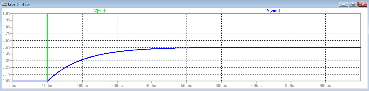
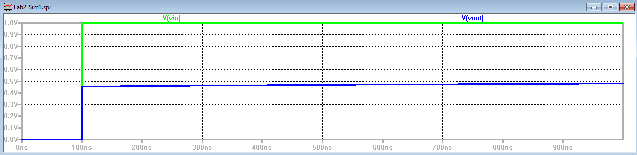
There is a delay when driving a capacitive load, as illustrated with our 10pF load. This charging delay will be the same as a standard RC circuit, Vin(1-e^(-t/RC)). Using the rule of thumb which is 0.7RC, we can see that it takes approximately 70ns to reach 50% charge.
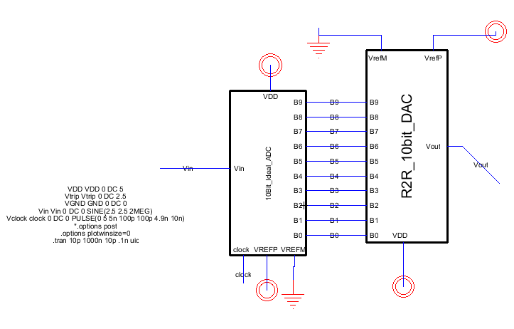
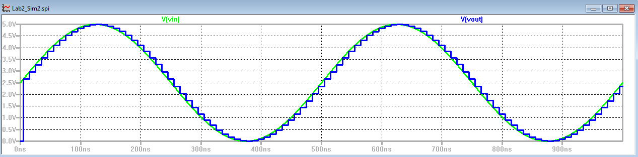
To show that the DAC is operating properly, we connect it to an ideal ADC and compare input to output voltages. The input to the ADC is a sinusoidal signal, which is converted into a 10-bit digital signal. This signal is directly transmitted to our DAC, which recreates the signal with discrete values, with a step size of (5/2^10) or slightly under 5mV. This simulation is less precise due to the clock speed.
To illustrate how the DAC responds to an RC load, we put a capacitor and resistor in series on Vout. This will create an RC effect on the output, which will slowly charge the capacitor but the voltage will increase to near peak levels quickly, due to the large resistor.
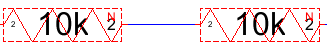
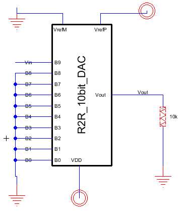
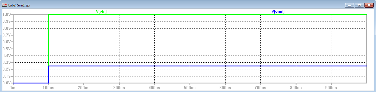
Problems can occur if the load resistance is too small, as it is comparible to the output resistance. As shown, output voltage will be half if the output load is a 10k resistor. As we determined earlier, the output resistance of the DAC is 10k, so with a load of 10k as well we will have half our expected output voltage. In the below example, we expect to have half our input voltage of 1v, which would be 0.5v. However, the simulation reveals that the true output voltage is 0.25v, half our expected value.
In a real system, the switches that control our DAC inputs have a non-zero resistance. This can create problems, such as voltage drops that cause the output voltage to differ, as well as changing the output resistance which can influence load choices. These effects can be compensated, but first one must be aware of them.