Lab Project - ECE 421L
Authored
by Carlo Lopez-Tello.
Email: lopeztel@unlv.nevada.edu.
November 08, 2013.
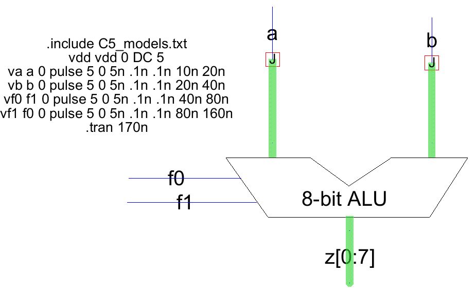
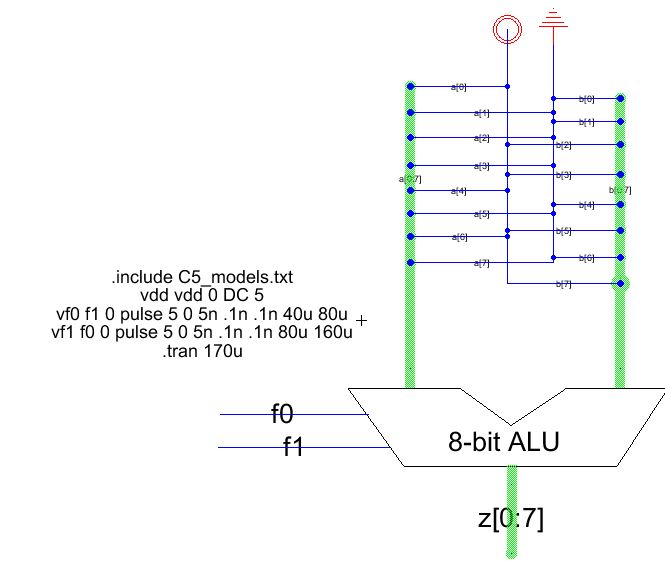
Design of an 8 bit ALU that has the follwoing operations: a OR b, a AND b, a + b, a-b.
This ALU needs two 8 bit inputs a and b, one 8 bit output z, and two 1-bit inputs f0 and f1.
The signals f0 anf f1 are used to select the mode of operation of the ALU.
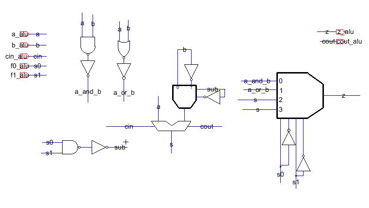
There are 5 components needed to make an ALU: OR gates, AND gates, inverters, 2to1 MUXes, and a full adder.
This is what a 1 bit ALU looks like.
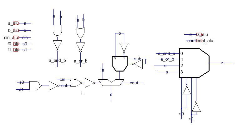
A 4 to 1 MUX is used to select the output. To do subtraction a 2 to 1 Mux is used to select b', and
Cin is set to one when both f0 and f1 are high.
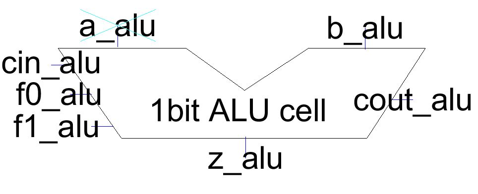
1bitALU_cell_icon.JPG
Icon for 1-bit ALU
Simulation of 1-bit ALU
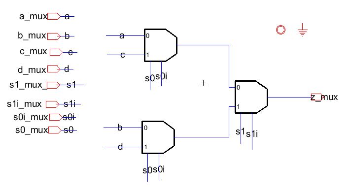
To make the 4 to 1 MUX we use two 2 to 1 MUXes.
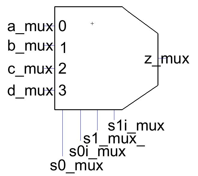
Icon for 4 to 1 MUX
Simulation of 4 to 1 MUX
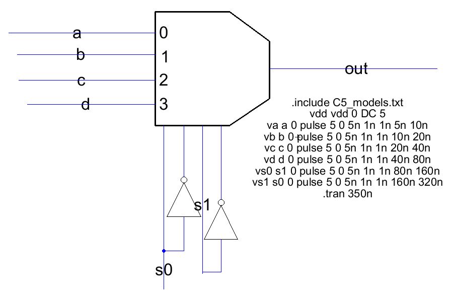
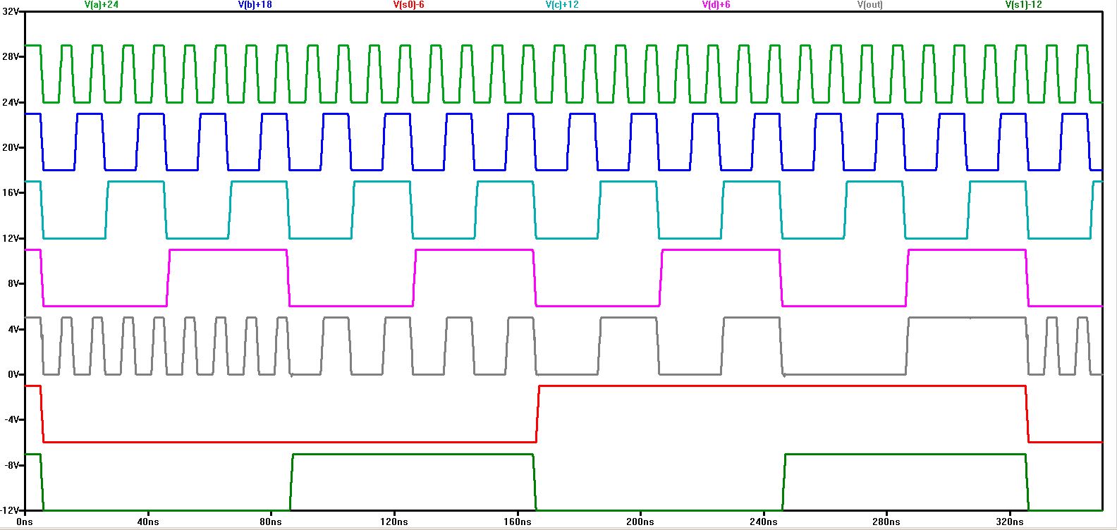
The bottom two signals are the select, and the one above them is the output. Notice that it matches the selected input.
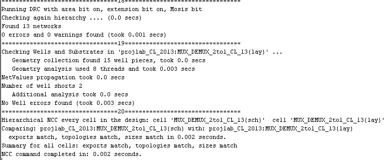
Since only the first Cin of the ALU has to be one when subtracting we can modify the 1-bit ALU so that we can use it
as a cell.
Icon for cell.
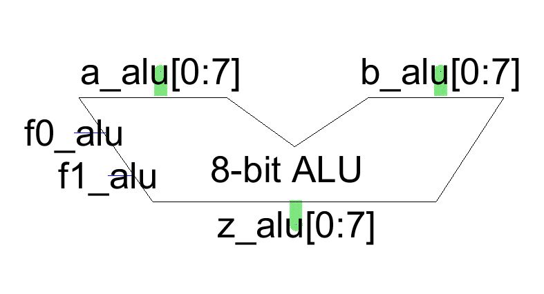
Now to make the 8-bit ALU.
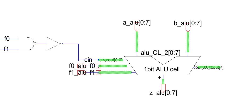
Notice that the first Cin is 1 when subtracting.
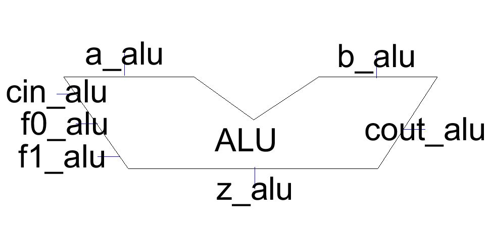
Icon
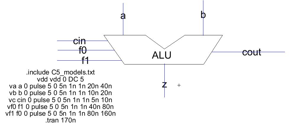
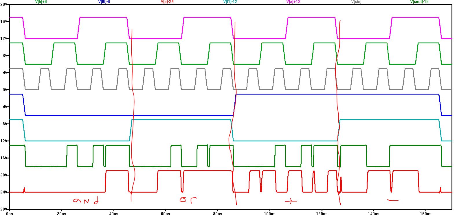
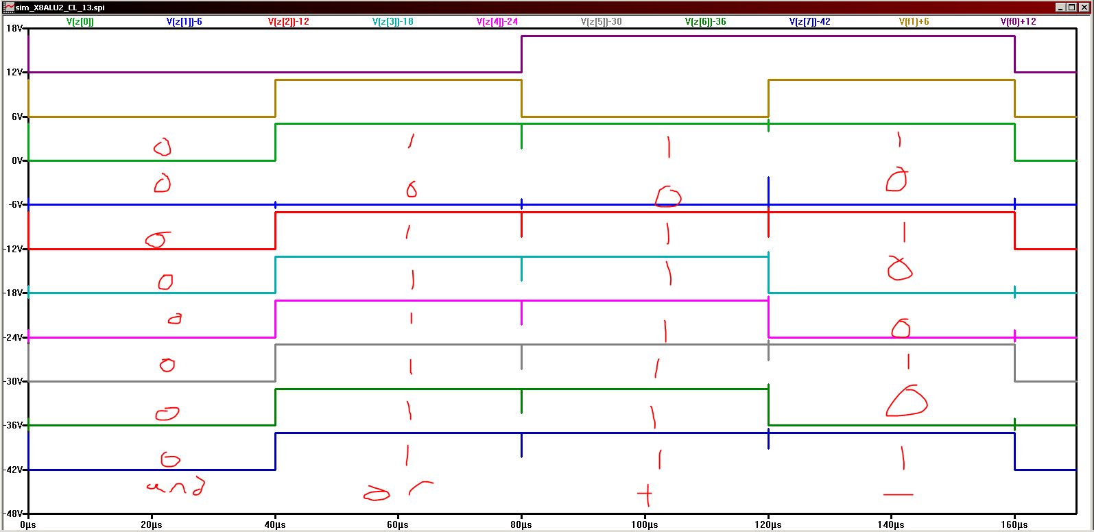
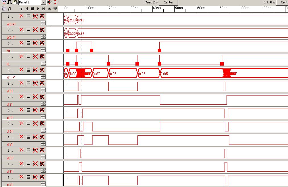
Simulations of ALU
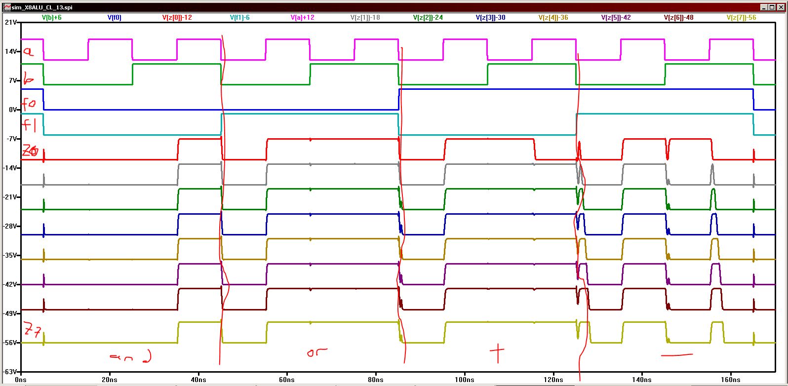
a = 01010001 b=10101100 a AND b = 00000000 a OR b = 11111101 a + b = 11111101 a-b = 10100101
Simulation using IRSIM
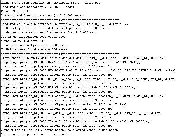
We need to layout the components of the ALU.
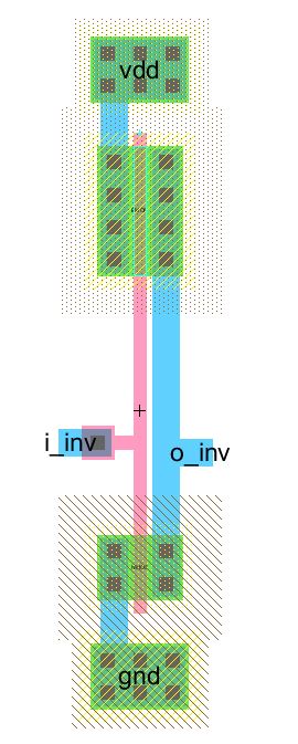
Layout of the inverter.
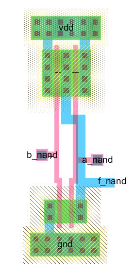
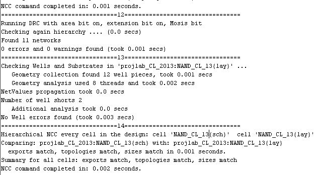
Layout of the NAND gate
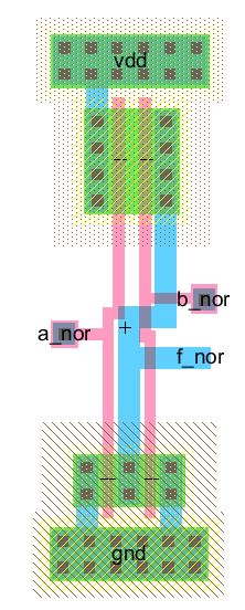
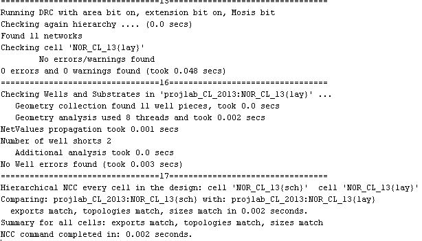
Layout of the NOR gate
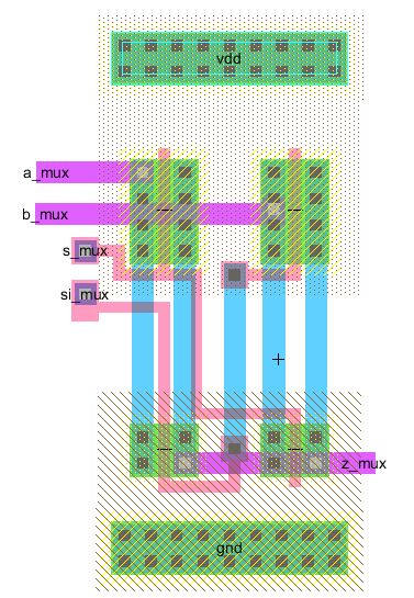
Layout of a 2 to 1 MUX
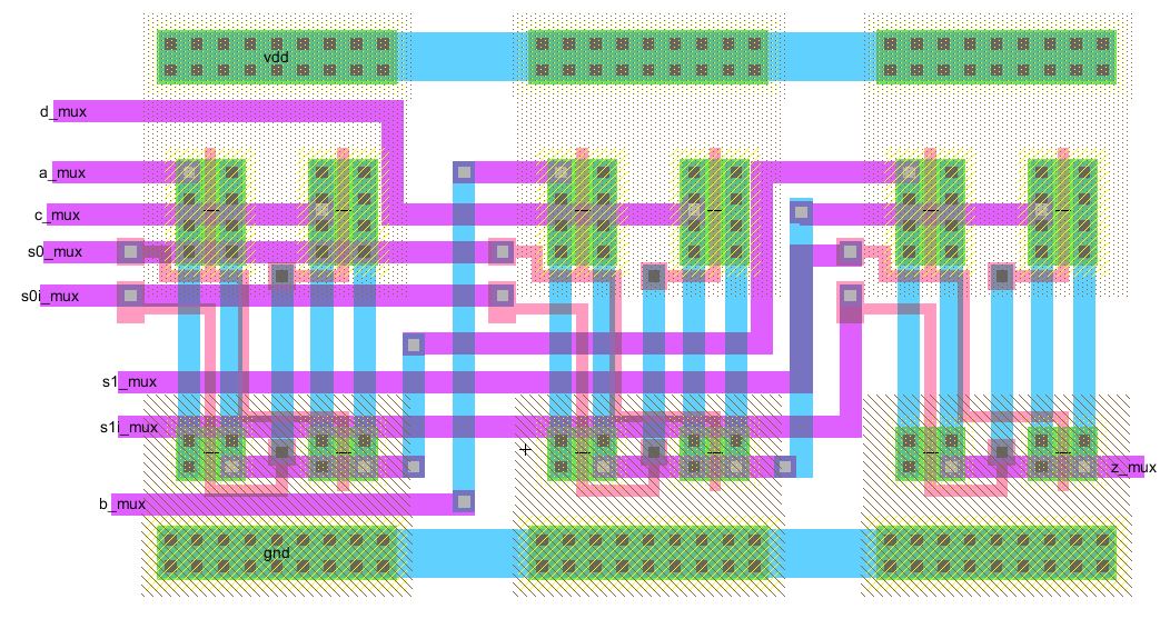
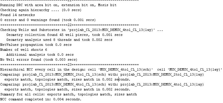
Layout of a 4 to 1 MUX
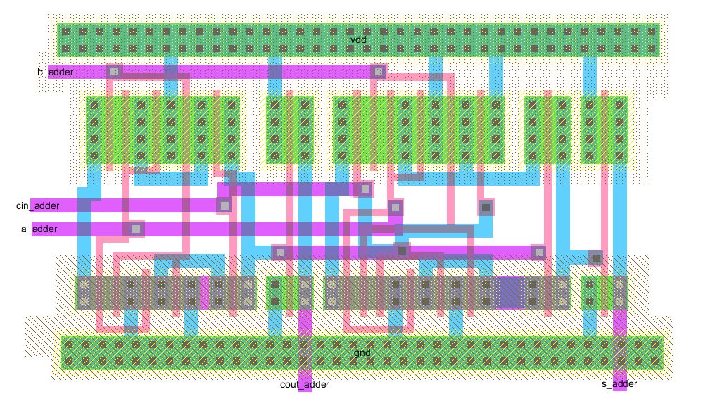
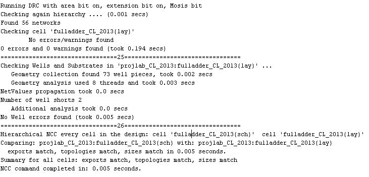
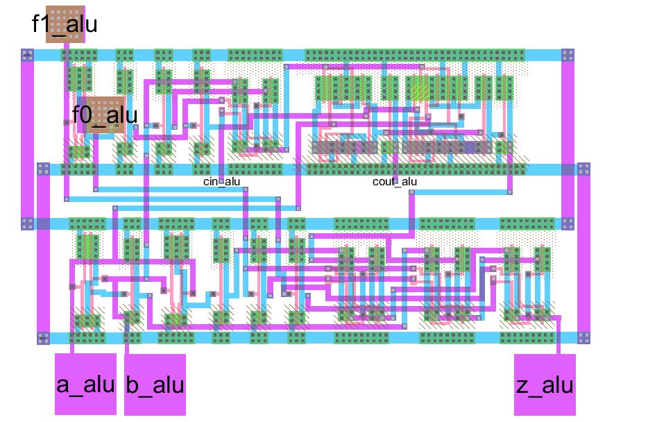
Layout of the full adder
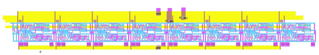
Layout of the alu cell

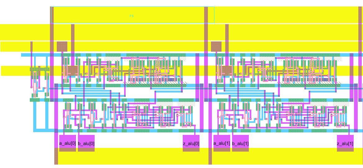
Layout of the 8 bit alu
Link to jelib.
Return to EE 421L Labs