Lab 7 - ECE 421L
Authored
by Carlo Lopez-Tello.
Email: lopeztel@unlv.nevada.edu.
November 2, 2013.
Lab Description:
In this lab we will make 8 bit gates and an 8 bit full adder.
First, copy the NAND gate we previosly made, and rename it NAND[0:7].
Naming the gate in this way creates 8 gates in parallel and the bus connection allows us to connect to all 8 gates.
Also add the following exports.
Make sure to use the bus and not wires.
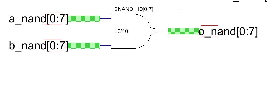
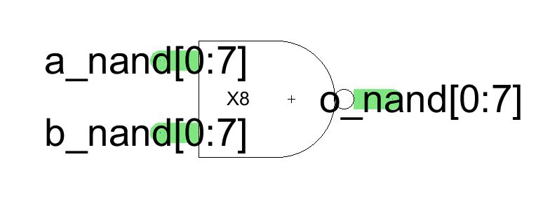
Make the following symbol to represent the 8 bit NAND gate.
Now, to make an 8 bit AND gate. Copy the NAND and the inverter and make the following schematic.
Make sure to use the bus and not wires.
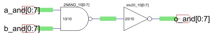
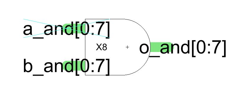
Make the following symbol to represent the 8 bit AND gate.
To make an 8 bit NOR gate. Copy the NOR and make the following schematic.
Make sure to use the bus and not wires.
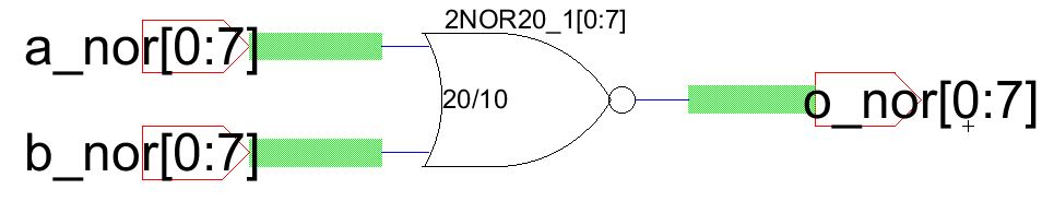
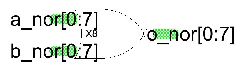
Make the following symbol for the 8 bit NOR gate.
To make an 8 bit OR gate. Use the NOR gate and inverter and make the following schematic.
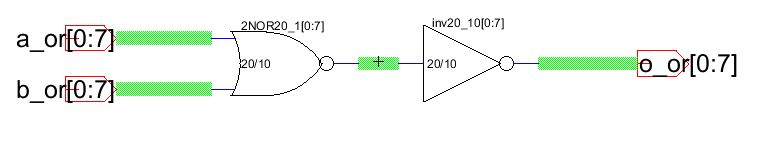
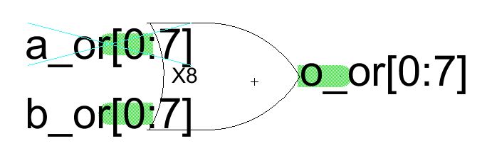
Make the following symbol for the gate.
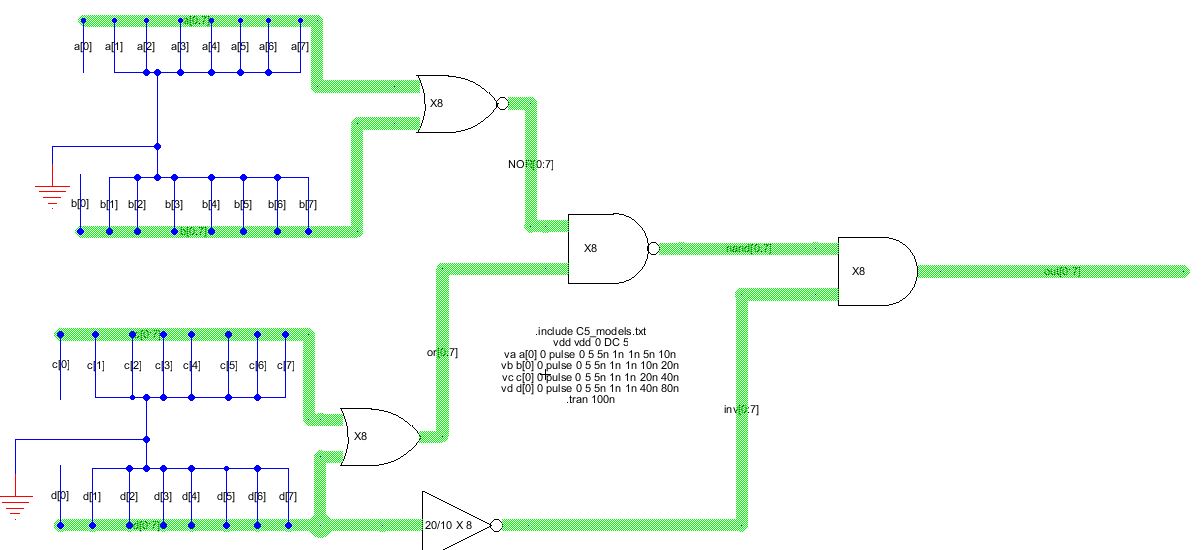
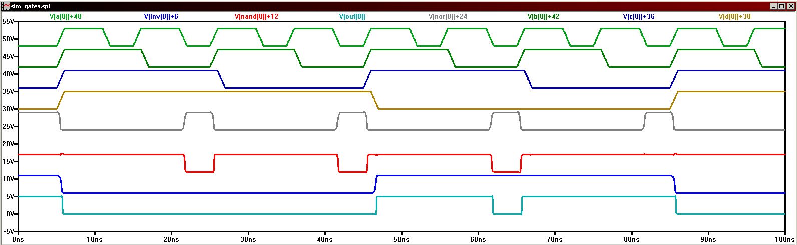
To make sure the 8 bit gates work were are going to build a logic circuit and simulate the gates.
Now we are going to make a MUX/DEMUX. A multiplexer is a logic circuit that takes multiple
inputs and outputs one of the inputs at a time depending on the select signal. A 2 to 1 MUX will have two inputs,
and one select, while a 4 to 1 will have 4 inputs and teo select select inputs. A DEMUX or de-multiplexer
simply reverses the operation of the multiplexer. So a DEMUX will take one input and output it to different
outputs depending on the select. The MUX and DEMUX circuits are identical what changes is the inputs and
outputs.
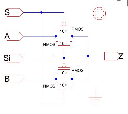
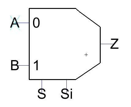
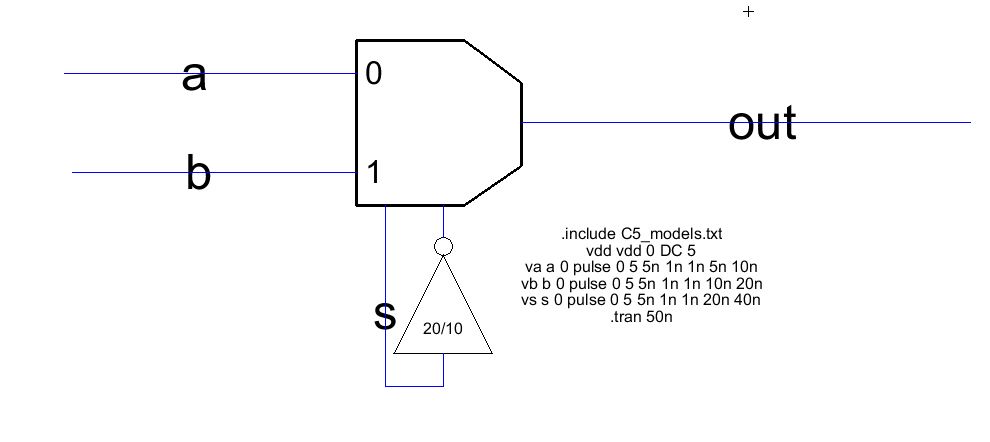
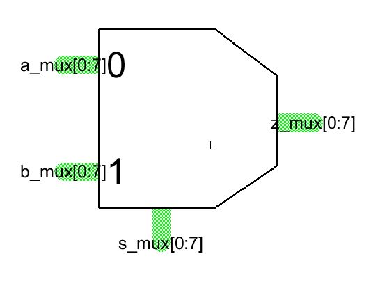
To make a MUX/DEMUX make the following schematic and symbol.
First we'll see how the circuit works as a MUX.
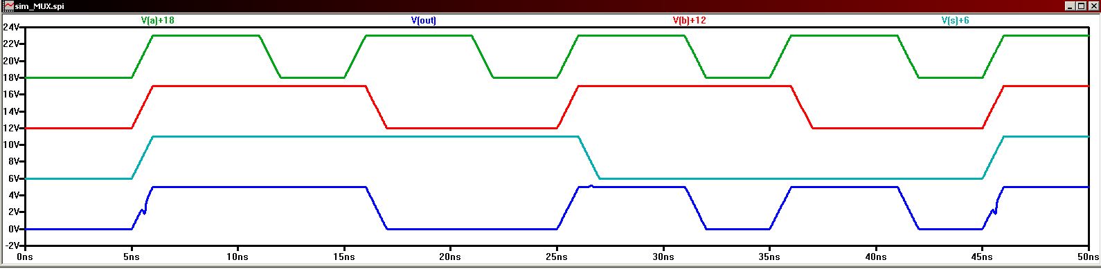
We can see the output change to the corresponding input line depending on the select.
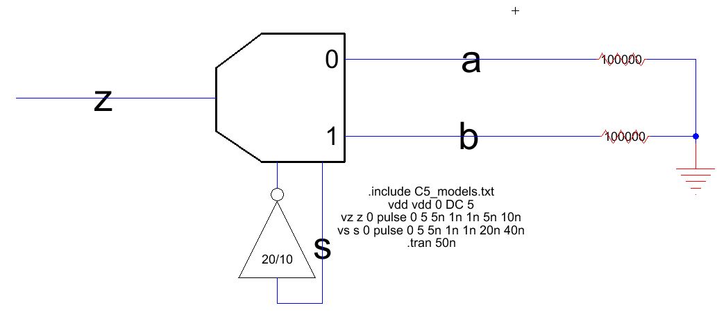
Now we'll see it wort as a DEMUX.
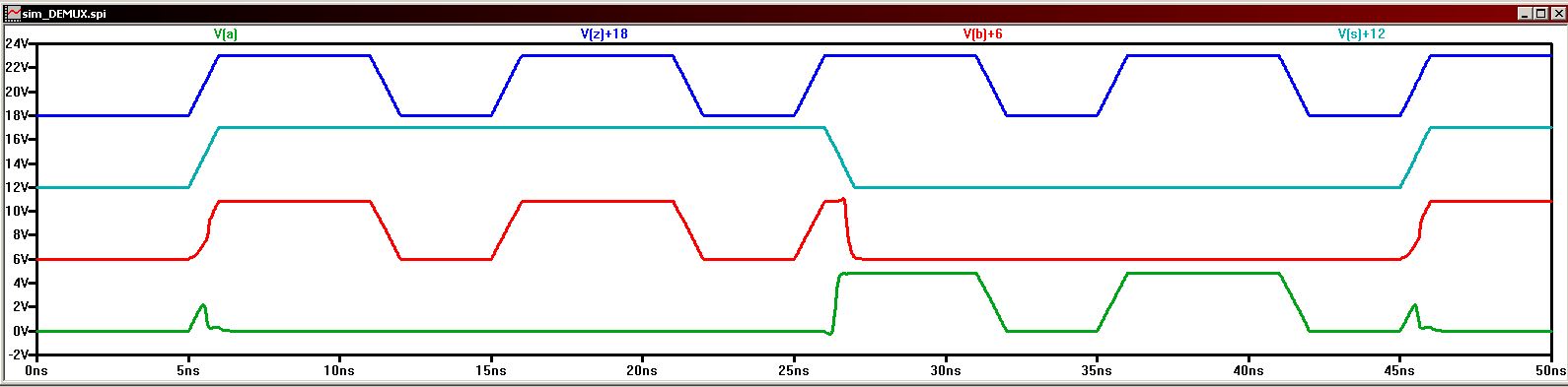
We can see the input signal switch between outputs depending on the select.
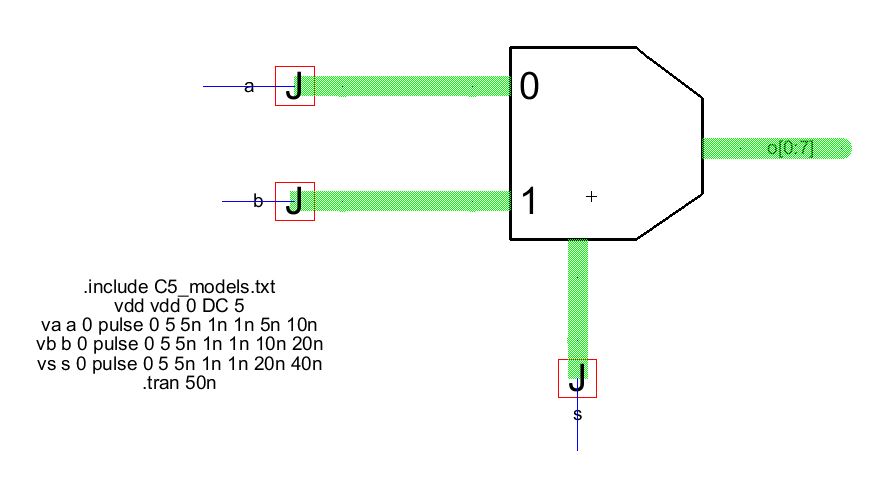
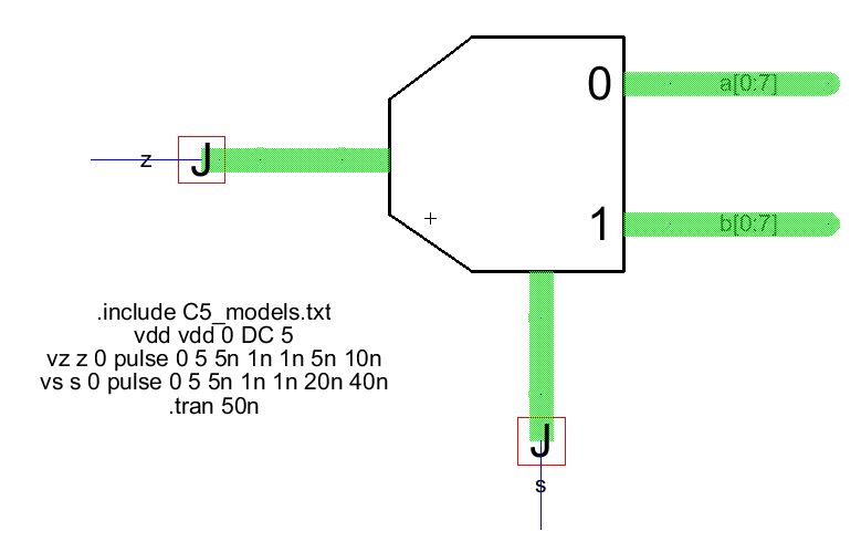
Now, we are going to make a 8 bit MUX/DEMUX.
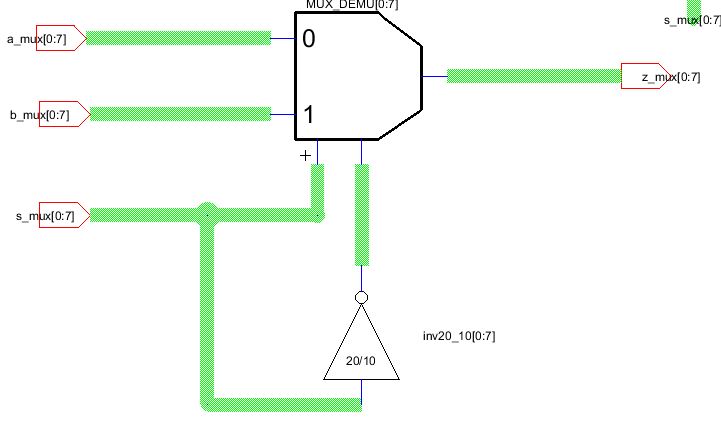
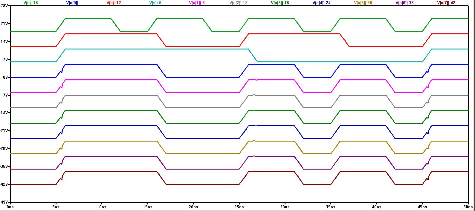
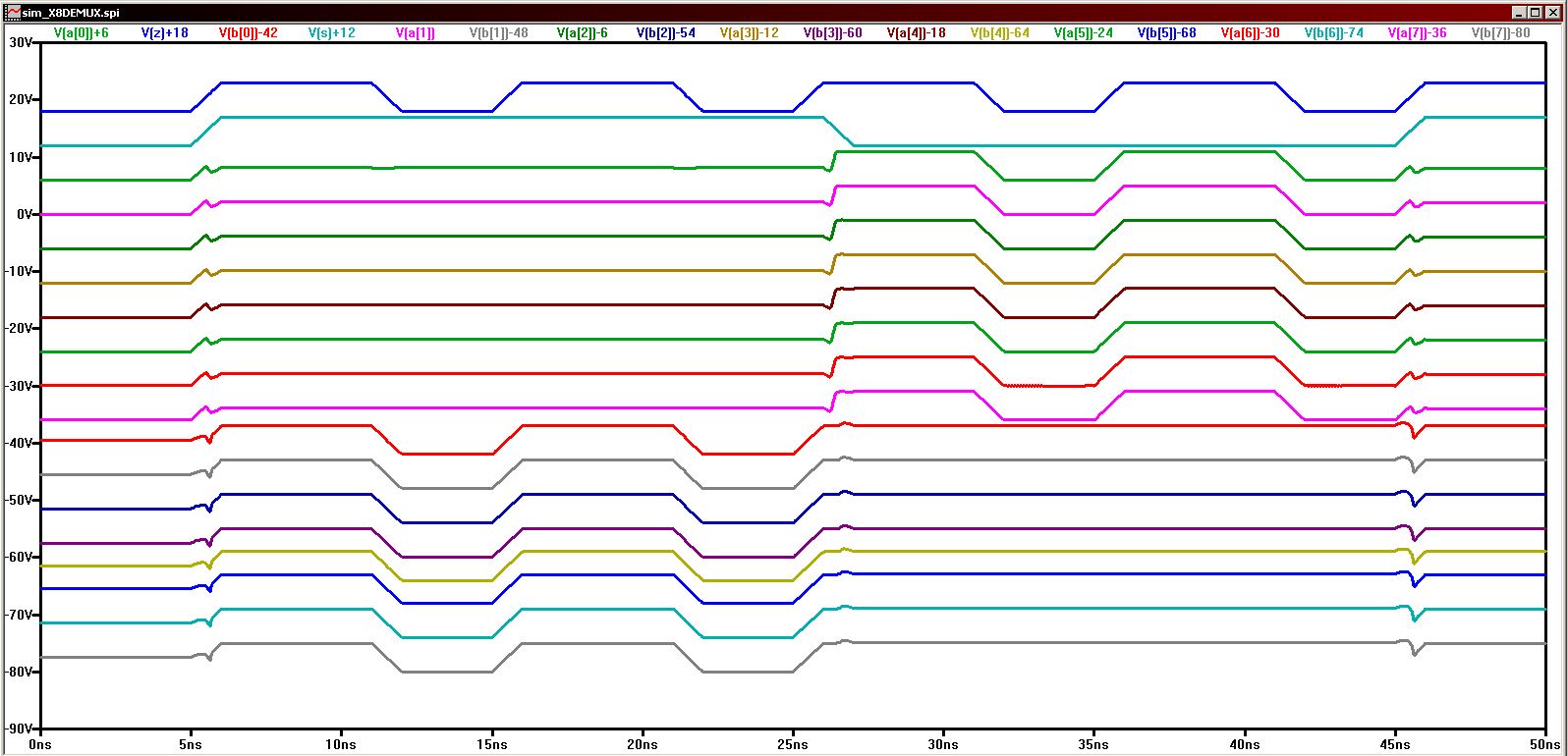
Now we'll simulate the 8 bit MUX/DEMUX
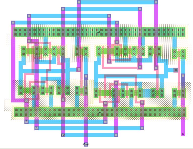
Next, we are going to make a full adder using the AOI configuration and 6 by two devices.
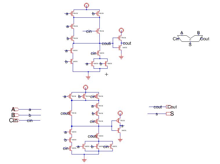
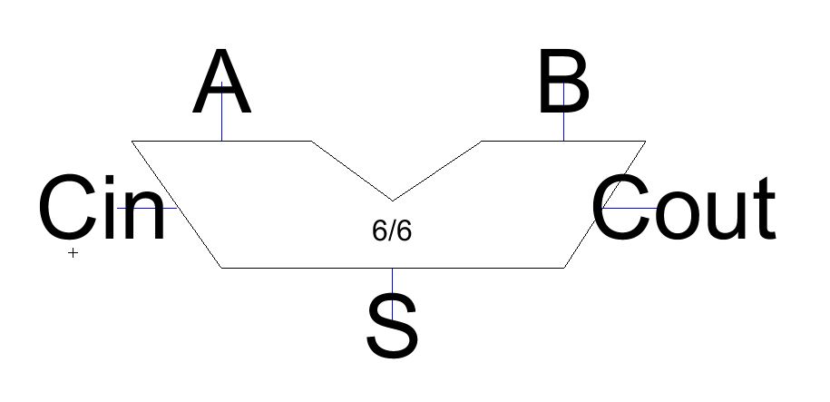
Make a symbol for the adder.
Layout the full adder.
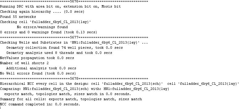
Check for errors: DRC, ECC, NCC.
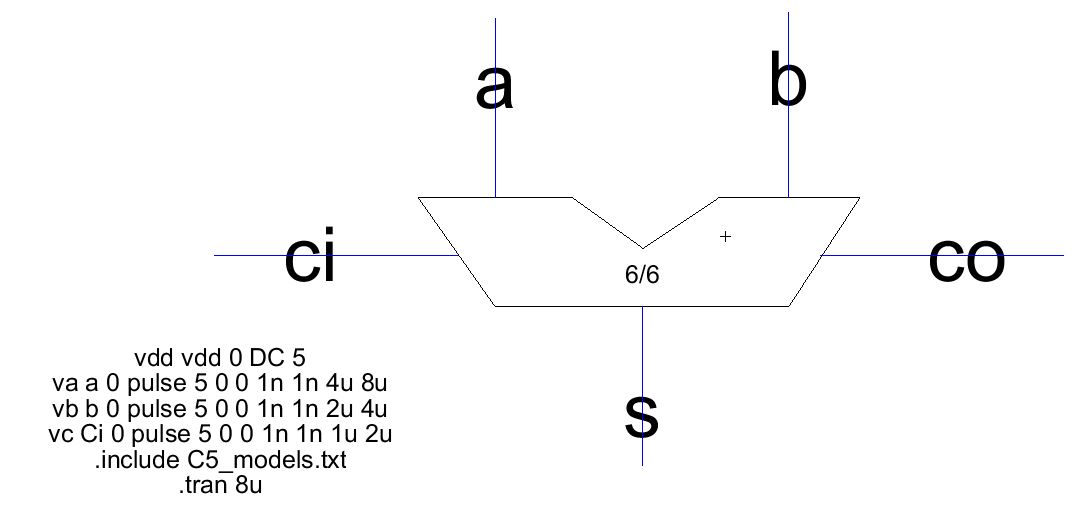
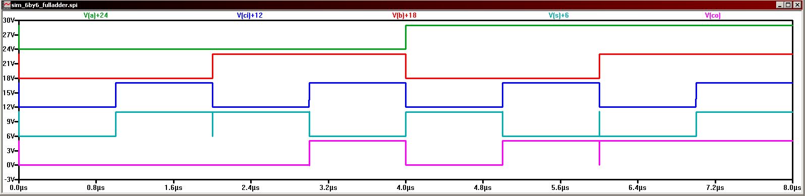
Simulate your design.
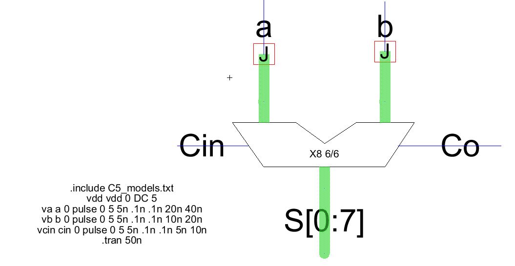
Finally, we are going to make an 8 bit full adder. Make sure eche carry feeds into the next. The cin and cout should be 1 bit.
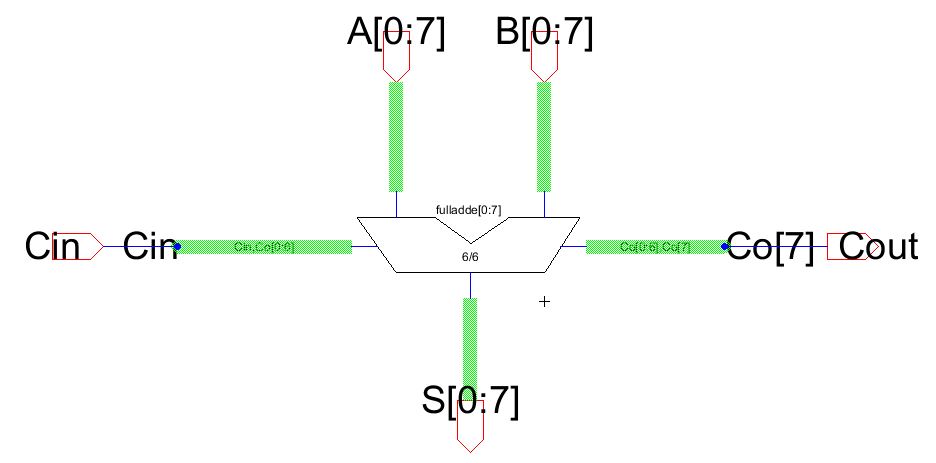
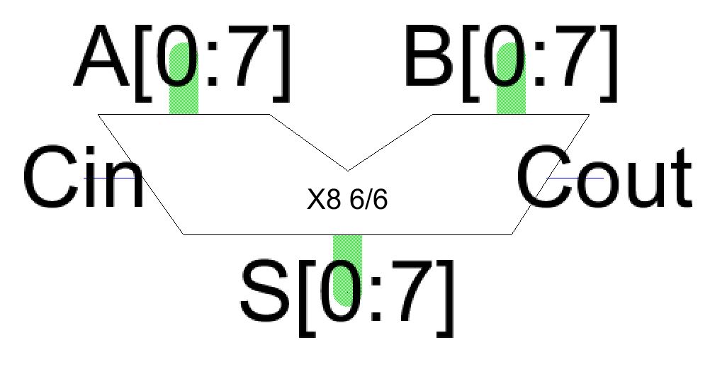
Make the following symbol for the adder.
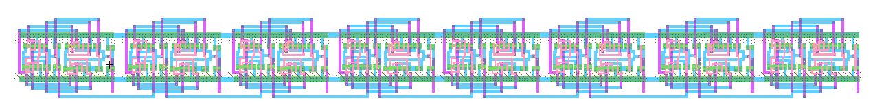
Use the layout for a 1 bit adder and copy it 8 times. Feed each cout to the next cin.
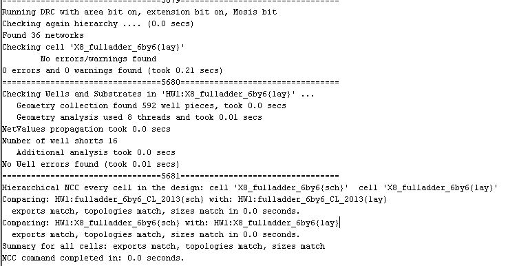
Check for Errors.
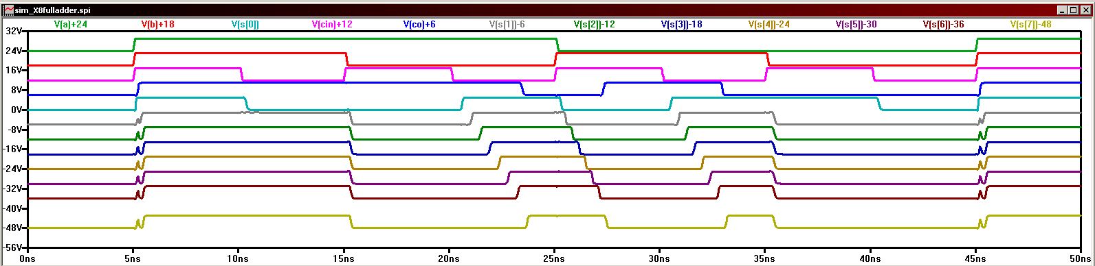
Simulate the 8 bit adder.
Backup your work.
Link to jelib.
Return to EE 421L Labs