Lab 6 - ECE 421L
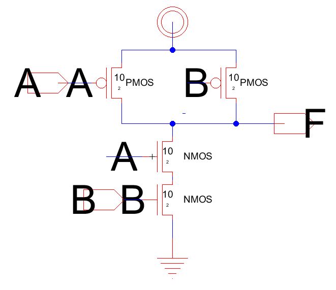
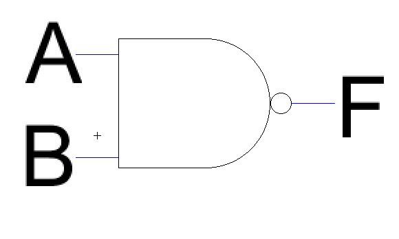
Make the following symbol to represent a NAND gate.
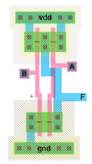
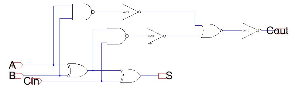
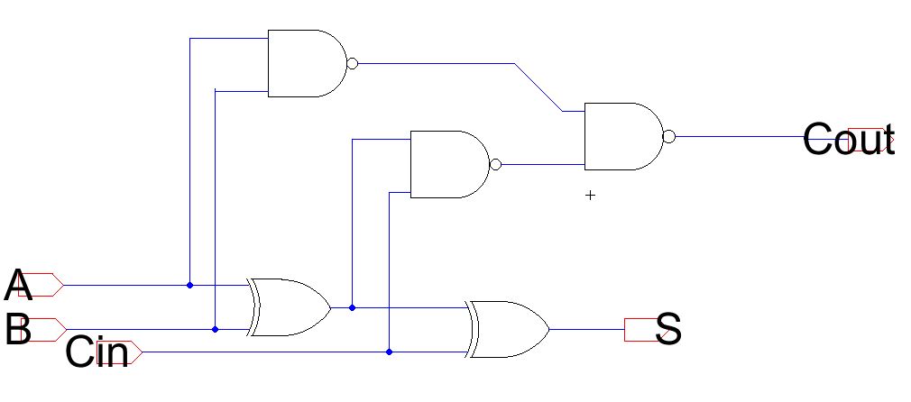
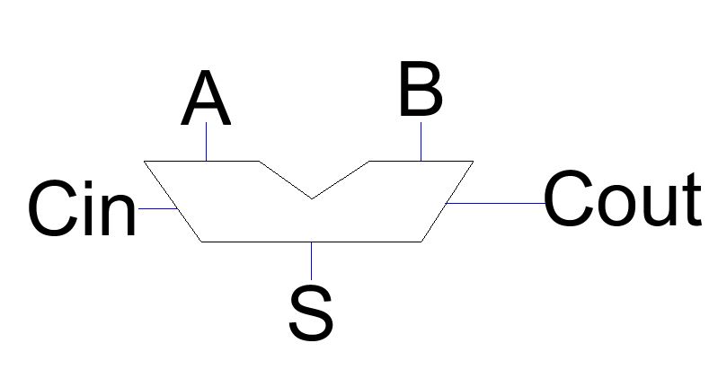
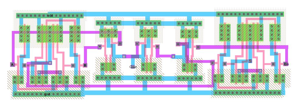
Finally, proceed to make the following layout.
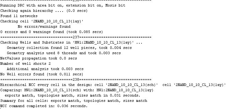
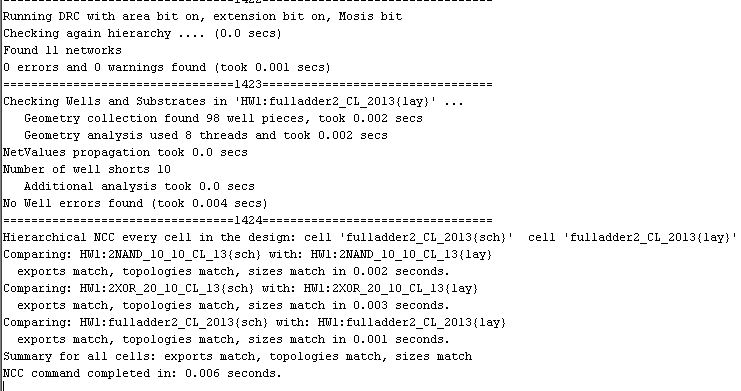
Check your layout: DRC, NCC, and ERC.
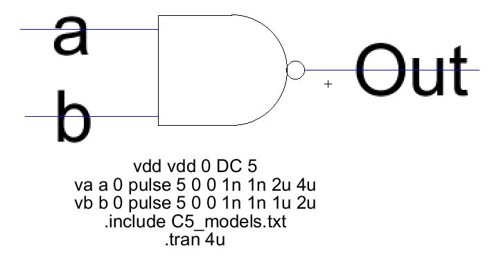
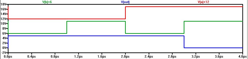
Now, we are going to simulate the operation of the gate using PSPICE.
Create a new schematic.
Make sure to increase the input voltages to make a display a better graph. Just add multiples of 6 to the inputs.
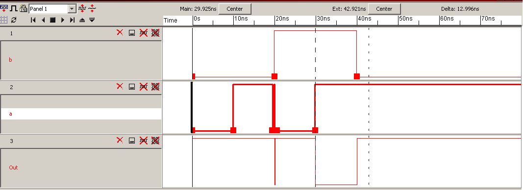
Now simulate the NAND gate using IRSIM.
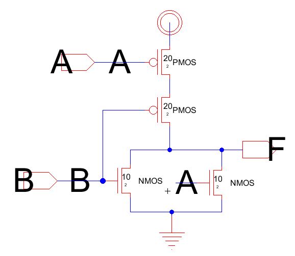
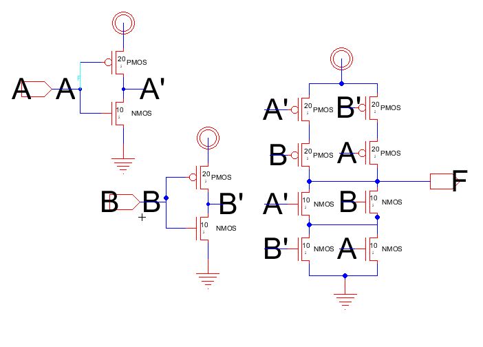
Make a NOR gate. A NOR gate consist of two NMOS and two PMOS in the following configuration.
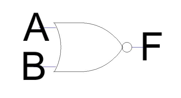
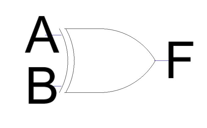
Make the following symbol to represent a NOR gate.
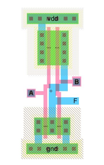
Finally, proceed to make the following layout.
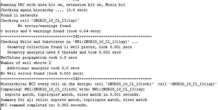
Check your layout: DRC, NCC, and ERC.
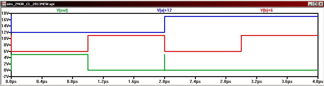
Now, we are going to simulate the operation of the gate using PSPICE.
Create a new schematic.
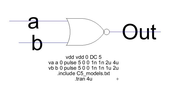
Make sure to increase the input voltages to make a display a better graph. Just add multiples of 6 to the inputs.
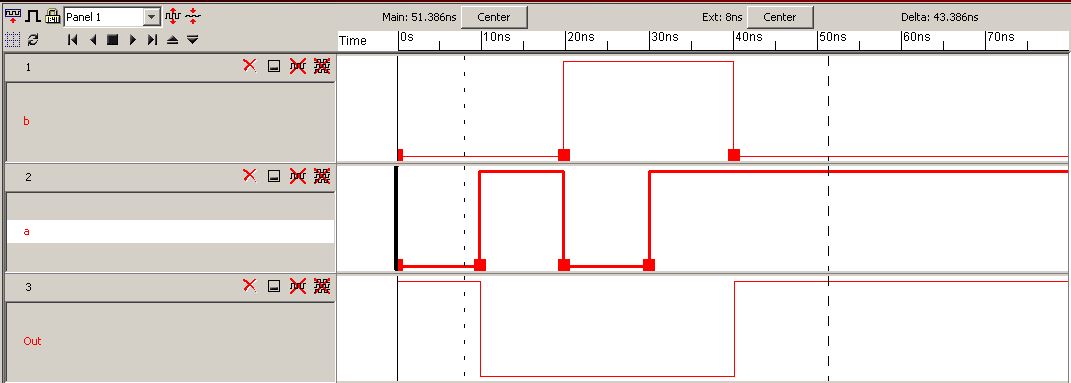
Now simulate the NOR gate using IRSIM.
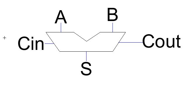
Make the following symbol to represent a XOR gate.
Finally, proceed to make the following layout.
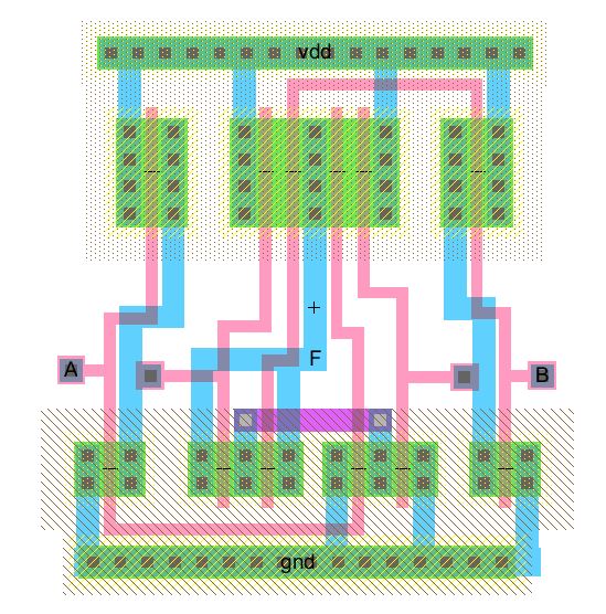
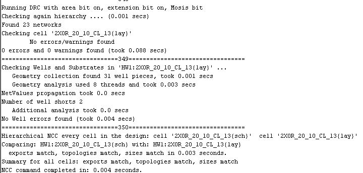
Check your layout: DRC, NCC, and ERC.
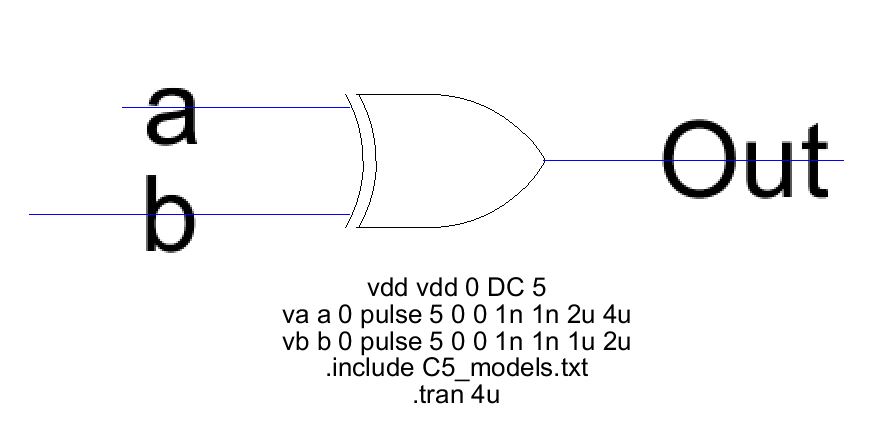
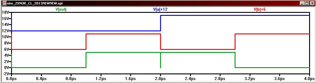
Now, we are going to simulate the operation of the gate using PSPICE.
Create a new schematic.
Make sure to increase the input voltages to make a display a better graph. Just add multiples of 6 to the inputs.
Now simulate the XOR gate using IRSIM.
Check your layout: DRC, NCC, and ERC.
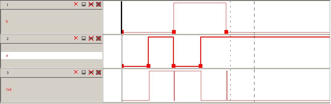
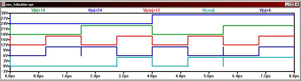
Now, we are going to simulate the operation of the adder using PSPICE.
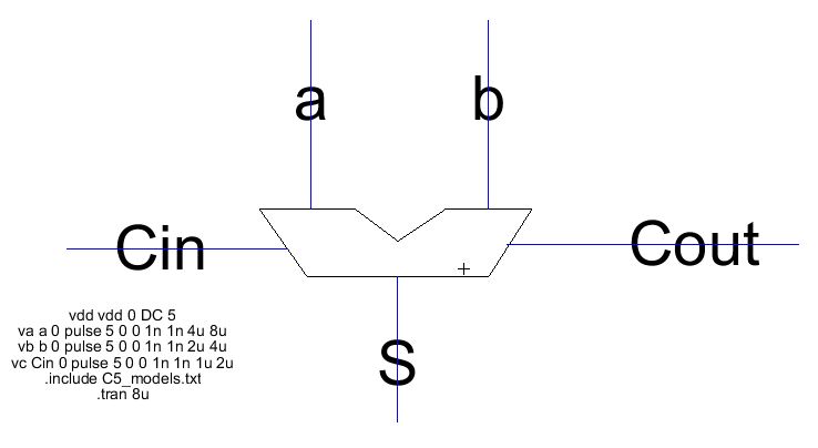
Create a new schematic.
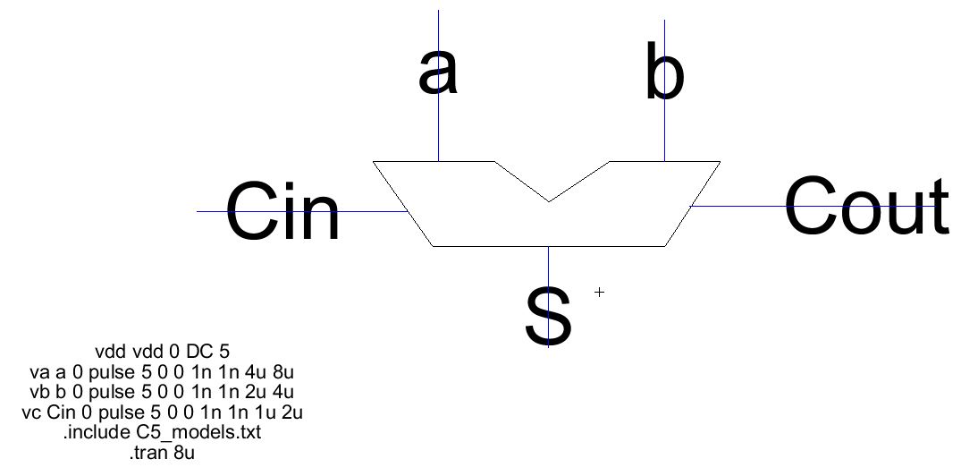
Make sure to increase the input voltages to make a display a better graph. Just add multiples of 6 to the inputs.
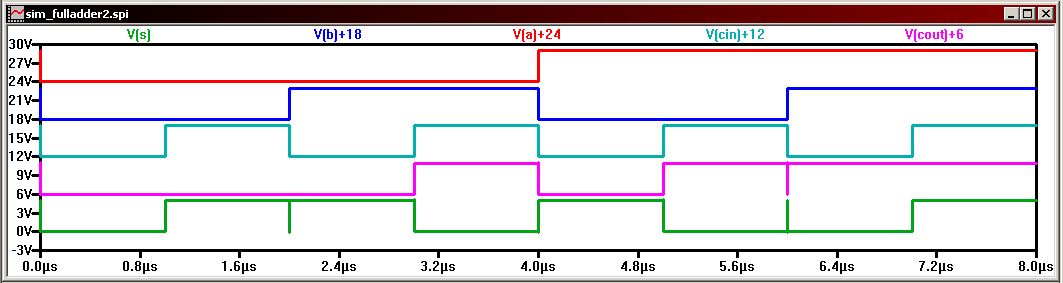
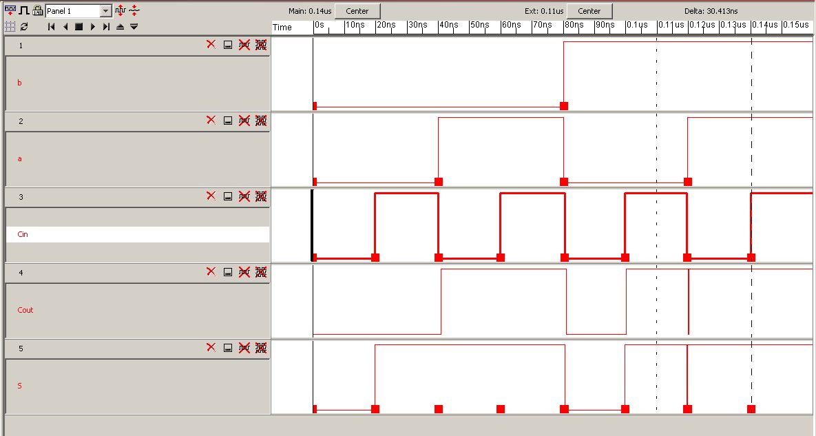
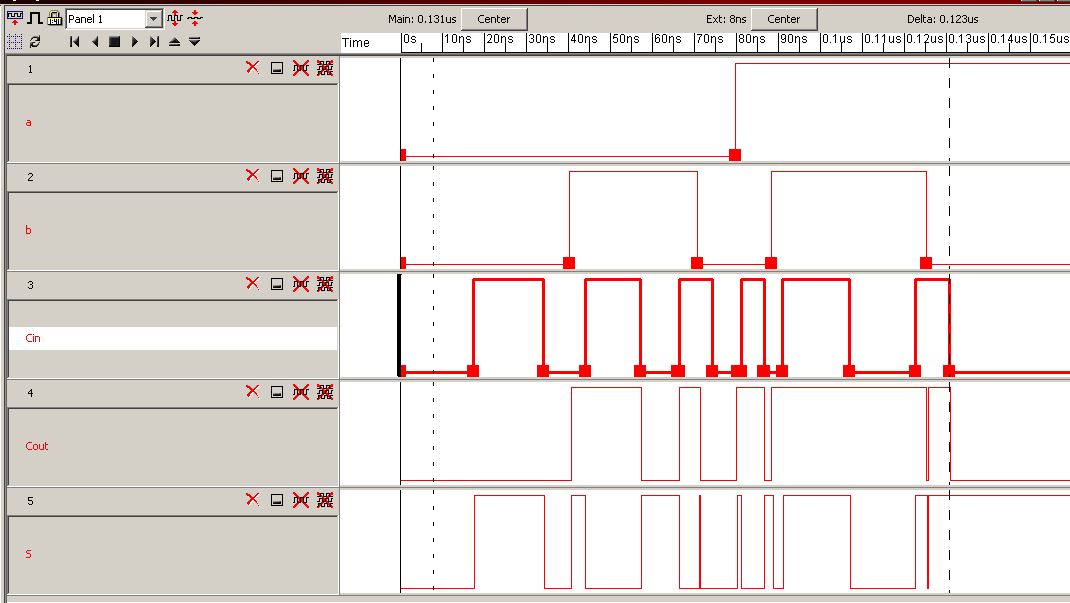
Now simulate the adder gate using IRSIM.
Backup your work.