Lab 5 - ECE 421L
First, we need to make the schematic, so create a new cell.
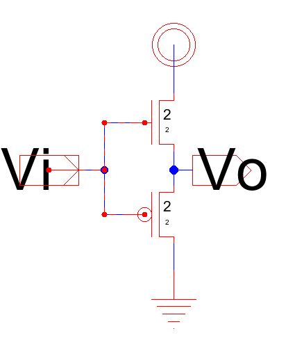
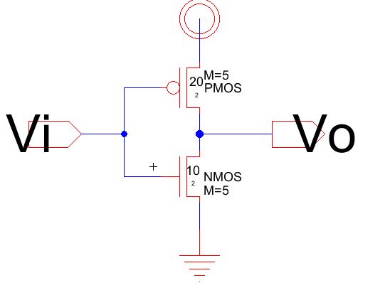
Select the a NMOS device and PMOS device and connect them in the following way. Remember to export the off-page nodes.
Change the width of the PMOS to 20 and NMOs to 10, and set their corresponding spice models.
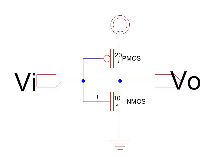
Create the following schematic for the inverter.
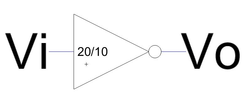
To make the symbol simply create a symbol cell with the same name as the schematic, or go to View>Make Icon View.
Make a new layout cell with the same name as the schematic cell.
The CMOS inverter is made of NMOS and PMOS transistors, so we need a NMOS node, a PMOS node, two N-active nodes,
two P-active nodes, a P-well node, and a N-well node.
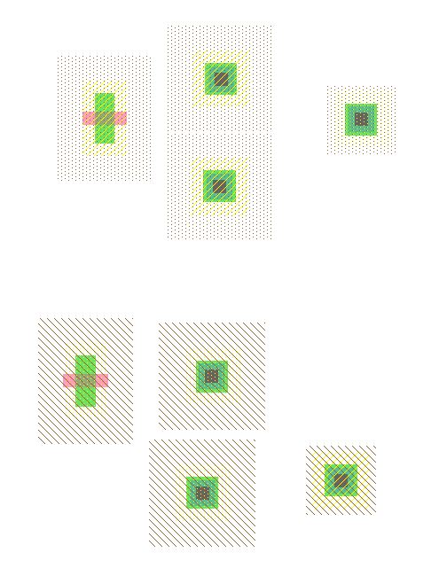
Change the width of the nodes match the schematic, and set the corresponding spice models.
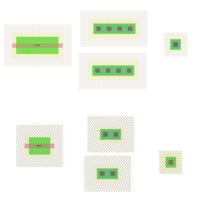
Make the NMOS and PMOS.
Now connect the parts to make the inverter. Make sure you export the same nodes in the schematic plus vdd and gnd.
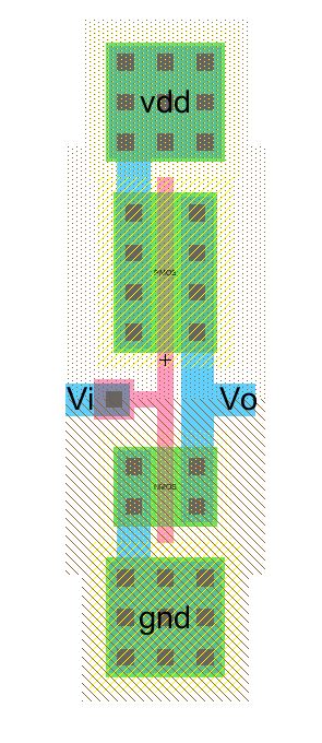
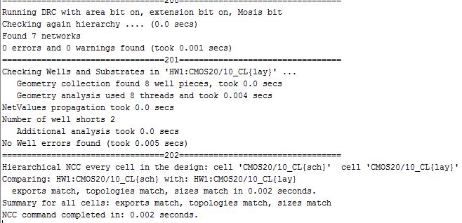
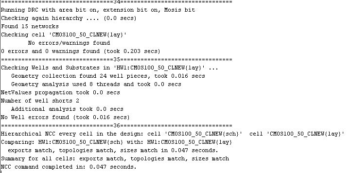
Check your layout: DRC, NCC, and ERC.
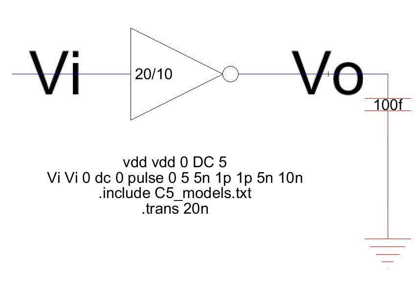
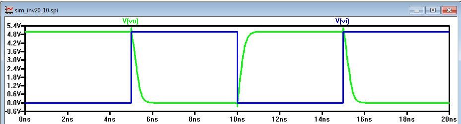
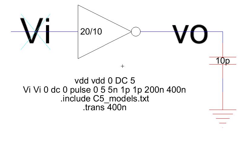
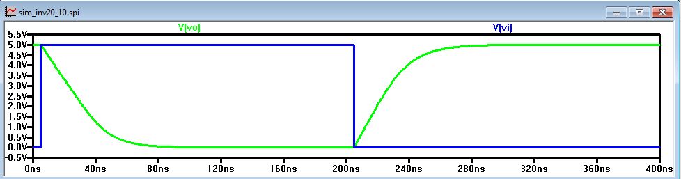
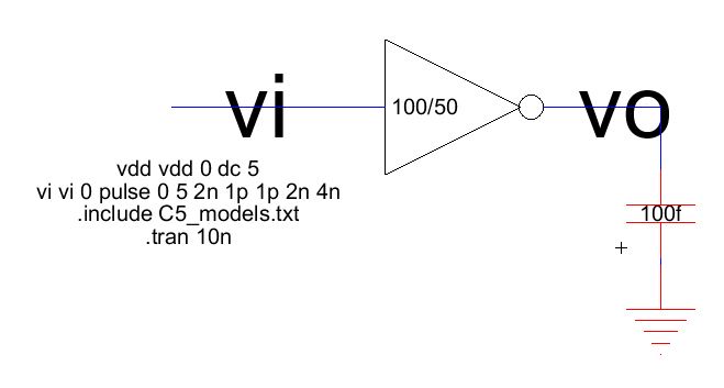
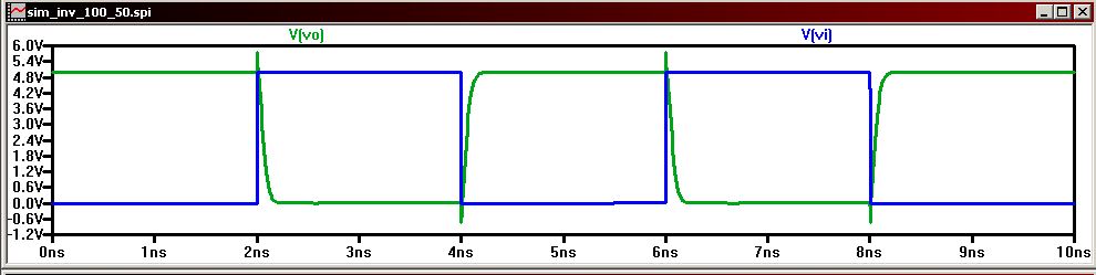
Now, we are going to simulate the operation of the inverter driving a 100f capacitor.
Create a new schematic, and add this file(C5_models.txt) to the same directory the jelib is in.
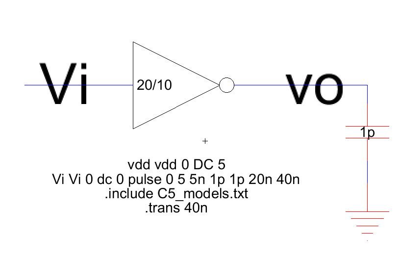
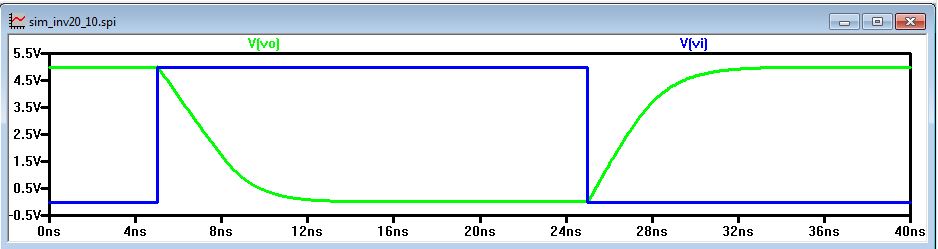
Driving a 1p capacitor.
Driving a 10p capacitor.
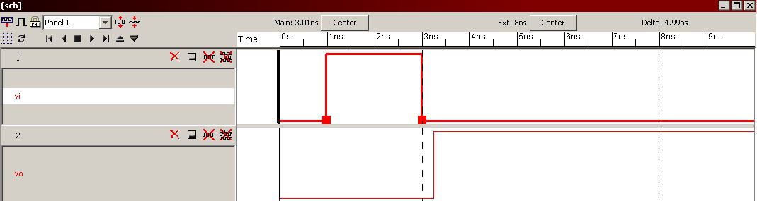
We can also simulate the inverter using IRSIM. First add offpage nodes to the schematic, make sure vin is an input and vo is an output.
Run IRSIM by going to Tools>Simulation(Built-In)>IRSIM: simulate current cell.
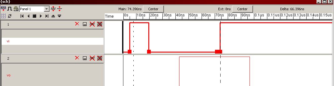
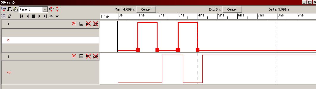
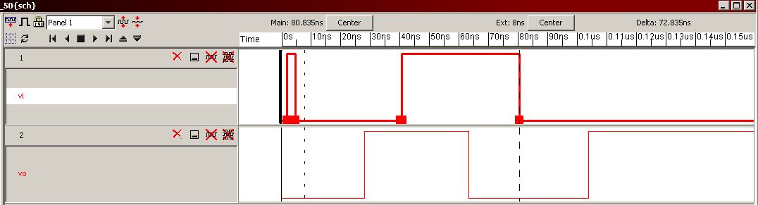
Driving a 100f capacitor.
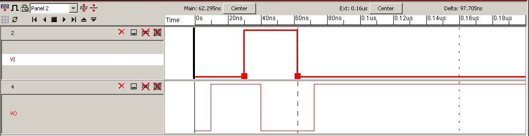
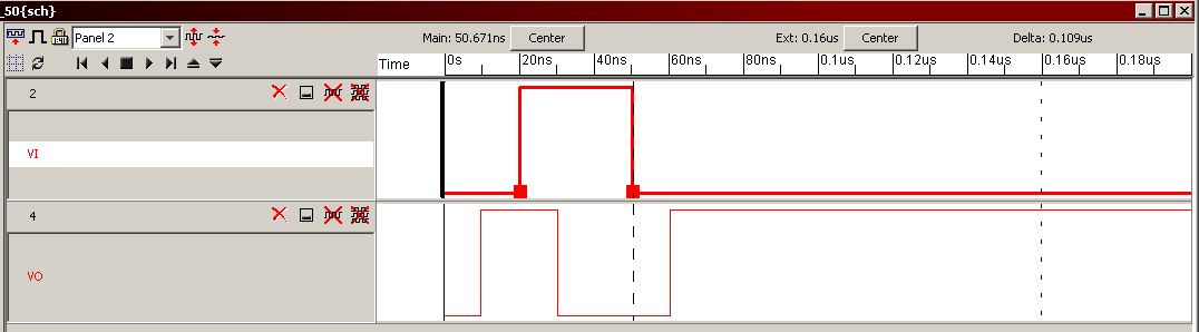
Driving a 1p capacitor.
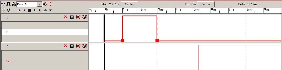
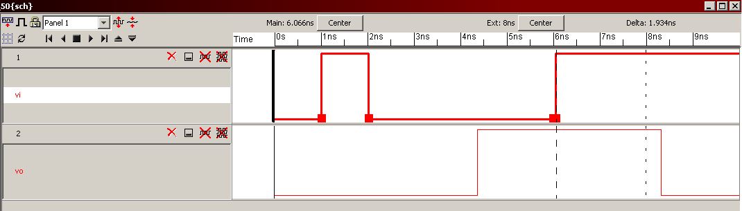
Driving a 10p capacitor.
Using ALS we can simualte logic, but not delays. To use ALS go to Tools>Simulation(Built-In)>ALS: simulate current cell.
ALS uses a 10 ns dealy for all logic.
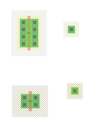
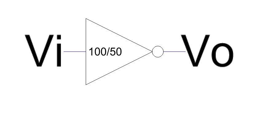
Now we are going to design a 100/50 inverter. First duplicate all the cells 20/10 inverter group.
The only modification needed in the schematic is a multiplier of five. To do this, select the PMOS and got to Tools>Simulation(Spice)>Add multiplier.
Add a multiplier of five to both NMOS and PMOS.
Make sure to change the text in yout symvol to 100/50.
To save area we can connect five 20/10 inverter in parallel instead of laying out a single 100/20 inverter.
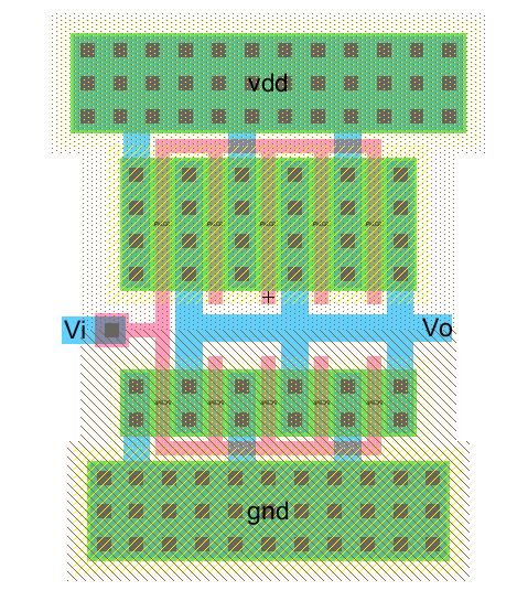
Check your layout: DRC, NCC, and ERC.
Just like before we are going to simulate the inverter driving 100f, 1pf, and 10pf loads.
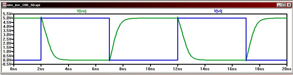
Driving a 100f capacitor.
Driving a 1p capacitor.
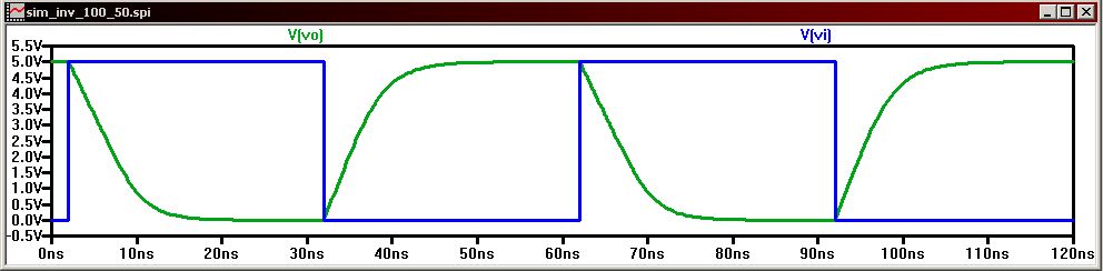
Driving a 10p capacitor.
Using IRSIM.
Driving a 100f capacitor.
Driving a 1p capacitor.
Driving a 10p capacitor.
Using ALS.
Backup your work.