Lab 4 - ECE 421L
We'll begin with the NMOS.
First, we need to make the schematic, so create a new cell.
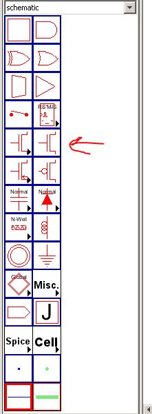
Select the NMOS device.
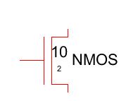
Change the width to 10 and set the model by going to Tools>Simulation(Spice)>Set Spice Model.

Click on "SPICE-Model" and change it to "NMOS".
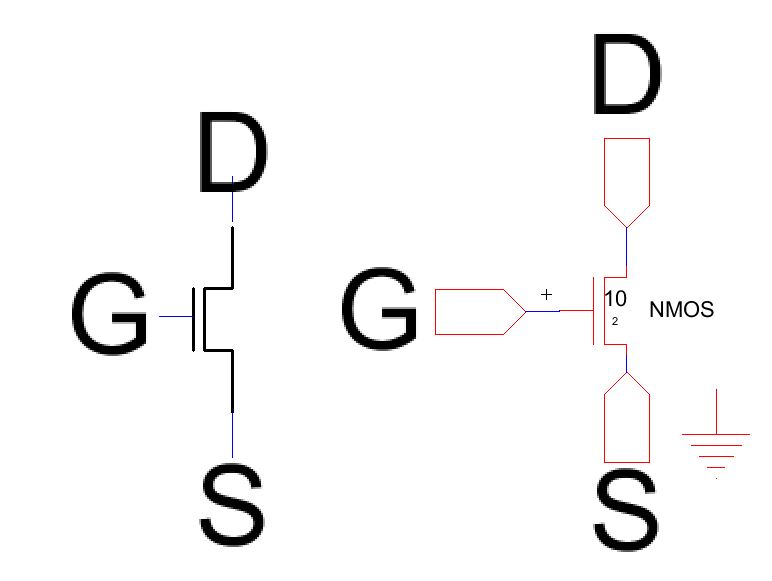
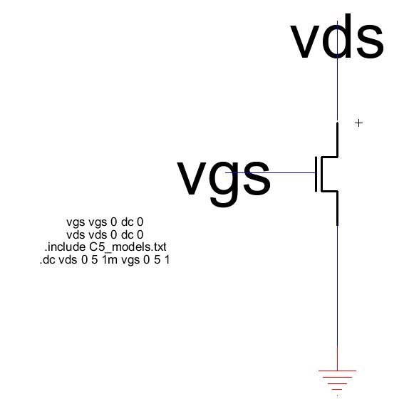
Create the following schematic for the NMOS.
To make the symbol simply create a symbol cell with the same name as the schematic, or go to View>Make Icon View.
Make a new layout cell with the same name as the schematic cell.
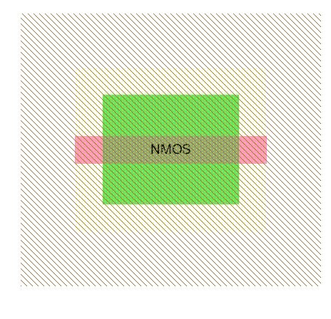
The NMOS is made of poly between two N+ regions. Therefore, select a NMOS node, two N-active nodes, and one Pwell node for ground.
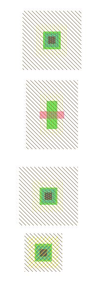
Change the width of the nodes to 10 to match the schematic.
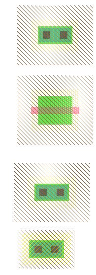
Set the spice model of the NMOS node to match the schematic.
Now connect the parts to make the NMOS. Add metal-1 connections, and export them to match the schematic.
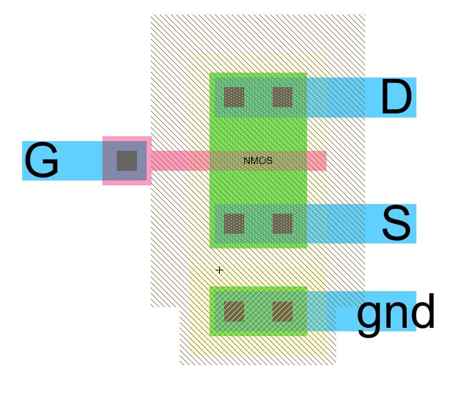
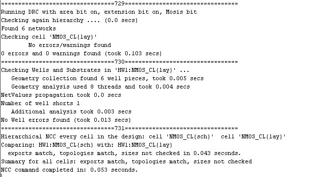
Check your layout: DRC, NCC, and ERC.
Now, we are going to simulate the I-V characteristics of this NMOS.
Create a new schematic, and add this file(C5_models.txt) to the same directory the jelib is in.
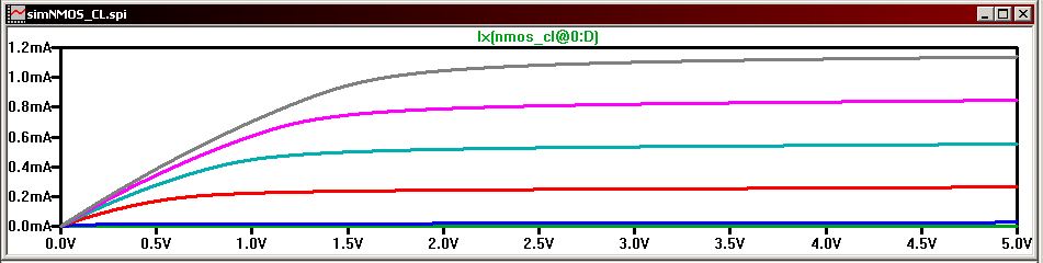
The current from vds to ground should look like this.
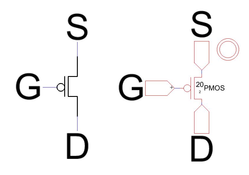
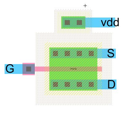
Now, we are going to layout a PMOS transistor. The schematic should look like this. remember to set the spice model to "PMOS"
and to change the width to 20.
Create a new layout cell with the same name. The PMOS is made of poly between two P+ regions, so select a PMOS node,
two P-active nodes, and a N-well node for VDD.
Change the width of the nodes, then connect the together ot make the PMOS. Remember set the Spice model,
and export the metal connections to match the schematic.
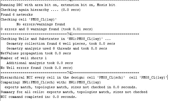
Check your design for errors: DRC, ERC, and NCC.
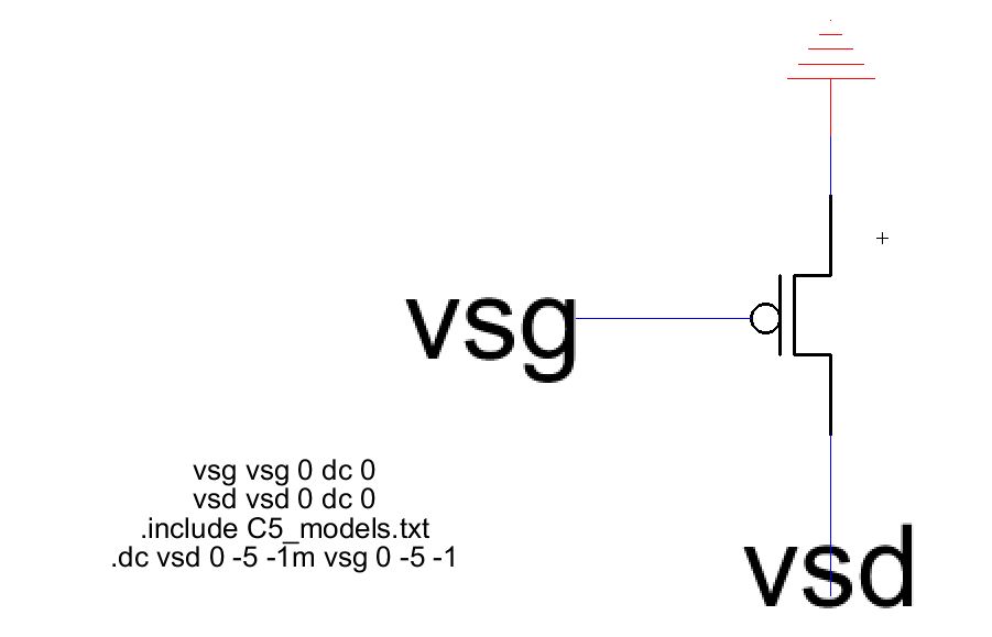
Create a shematic to simulate the PMOS I-V characteristics.
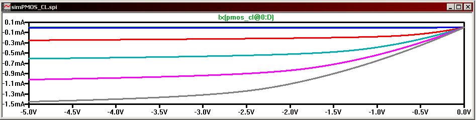
The current from vsd to ground should look like this.
Backup your work.