Lab 2 - ECE 421L
Download the lab2.jelib file. Then open both libraries in Electric by clicking on File>Open Library.
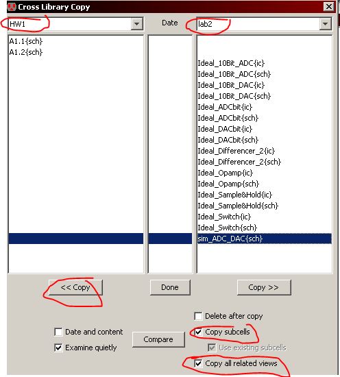
Copy the sim_ADC_DAC{sch} cell from the lab2.jelib library to your library by clicking on Cell>Cross-Library Copy.
Select your library and the lab2.jelib. Click on the sim_ADC_DAC{sch}, make sure Copy subcells and Copy all related, and click copy.
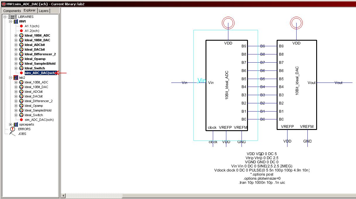
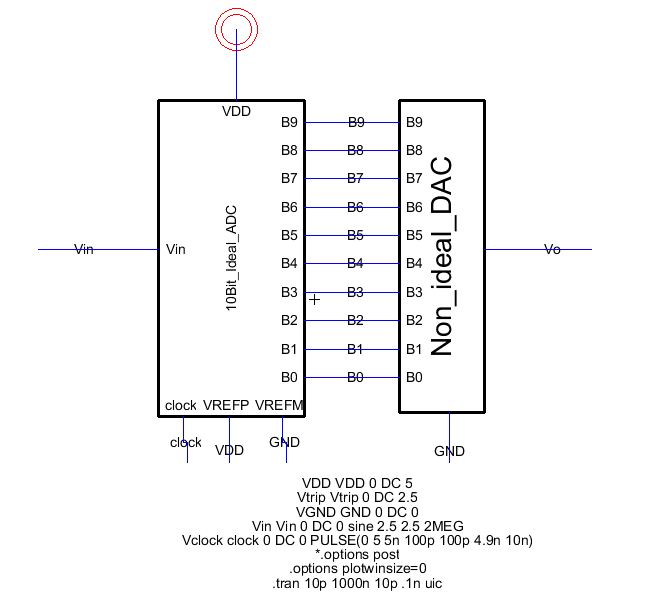
Open the sim_ADC_DAC cell by double clicking it. Proceed to run the simulation.
Simulation:
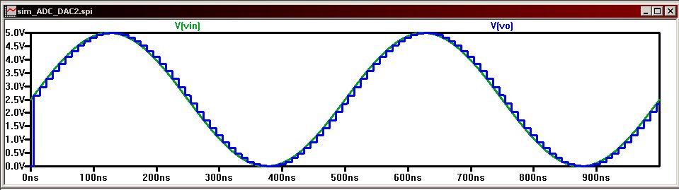
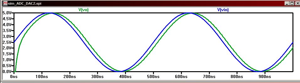
The ADC is converting the sine wave into a combination of bits. Using a simple example imagine a 1-bit ADC using some voltage Vref.
The ADC has to represent Vref using two values 0 and 1, so in this case whenever the input was higher than Vref/2 the ADC would
produce a 1 or 5 V output. Likewise when the input becomes smaller than Vref/2 the output is 0 V. Bigger ADCs work on the same principle,
but have a greater number of outputs to represent a smaller change in Vref.
ADCs can detect changes of Vref/2^N also called the least significant bit (LSB). 2^N is the total combinations a N-bit ADC can output, so the
lowest change in Vref that the ADC can detect is Vref/total combinations.
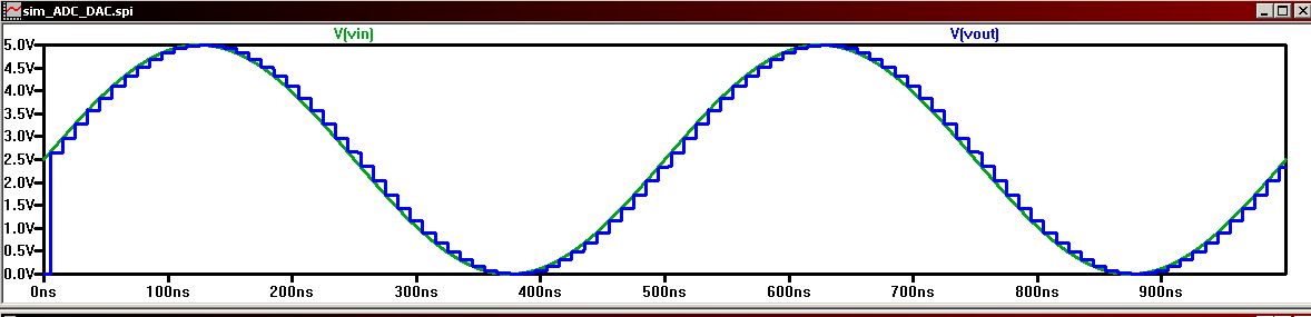
Given a 10-bit ADC using a 5V referece the LSB is 5/1024 = 4.88 mV. However, the simulation shows a change of output at 2.92 mV.
This does't mean the simulation or the calculation is wrong. The output of this ADC is shifted.
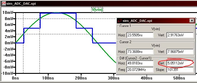
The shift is introduced to change quantization error from 1 LSB to +/-(1/2) LSB. Going back to a 1-bit ADC by shifting the output
a value from 0 to Vref/4 would produce 0, and a value from Vref/4 to 3Vref/4 would produce a 1. The last quarter is considered out of range
because we only have two combinations.
If we were to apply a voltage of 20mV then the output would be "100", because 20/4.88 = 4.
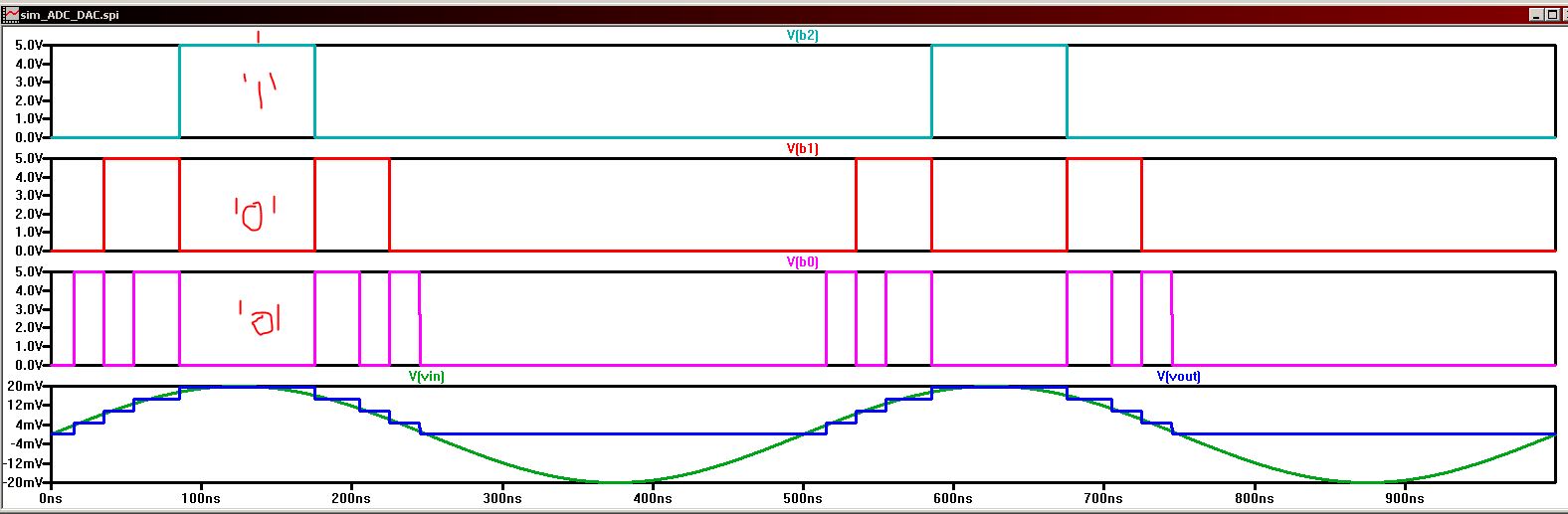
The DAC (Digital to Analog Converter) uses the bits generated by the ADC to recreate the input. One can think of the DAC as an multiplier.
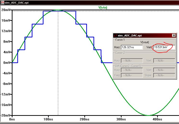
It multiplies the LSB by the number represented by its input. So if a 10-bit DAC gets "100" it will output 4*LSB = 19.52.
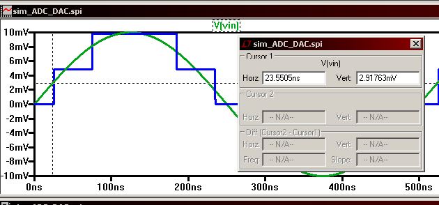
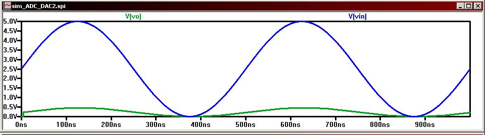
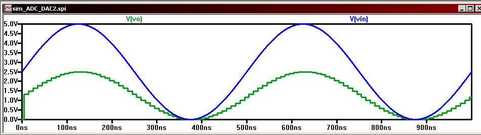
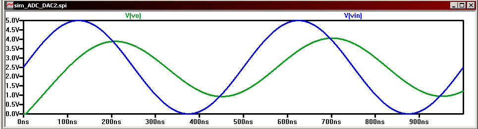
Same graph as above, but zoomed in on Vout.
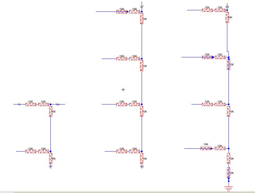
Now it's time to implement the following DAC. Create a new cell and build the following.

Your schematic should look like this.
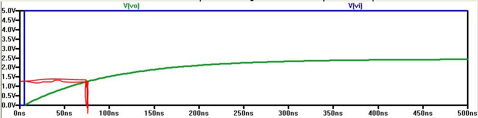
Test your circuit by grounding all inputs except B9. Then connect a pulse to B9 and simulate your circuit driving a 10pF load.
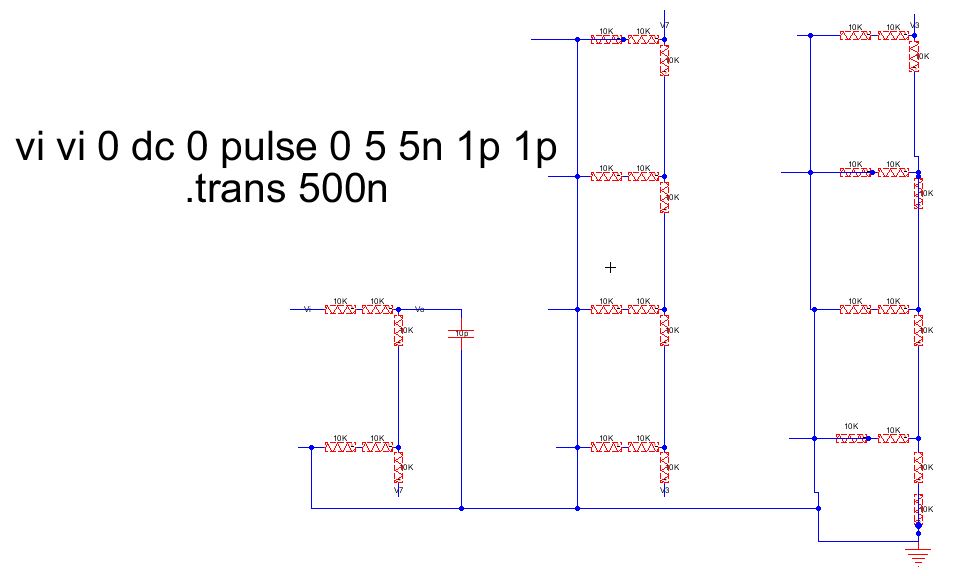
We can estimate the time it's going to take by finding the resistance and calculating .7RC. Going from the bottom to the top,
we can combine the resistors to calculate the output resistance of the DAC. The bottom node has two 20K resistors in parallel, which
equals 10k. The next node has 20k parallel to 10k plus the equivalent resistance from the bottom (10K). The combination of the second
brach equals 10k. Repeating this procedure, gives a total resitance of 10k. This means that when all nodes are grounded Vo is half of
Vin. When we connect our load the time it takes the capacitor to chage to 1.25V is .7*10p*10k = 70ns.
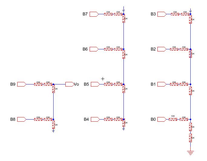
To create a new model first you need to add external ports. They are found in components above Spice.
To name them select a node and go to Export>Create New Export.
After adding the nodes and naming them, your schematic should look like this.
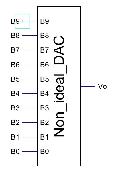
Now click on View>Make Icon View. This will create an icon that represents your schematic.
Open the model that was created to edit it to your liking. It should look something like this.
Duplicate the cell that has the simulation of ideal ADC and ideal DAC. Replace the ideal DAC with your own DAC.
Now try simulating your DAC.
The simualtion should look like this.
Now, try simulating the effect of different loads(R,C,RC) to see what happens.
With a load of 1K the output looks like this.
Load of 10k.
Load of 100k.

The DAC forms a voltage divider with the load, so if we want most of the voltage across the load we need it to have a greater
resistance.
A capacitive load of 1pF has the following effect.
Load of 10pF.
Load of 100pF.
A capacitive load add a phase shift to the output. The reason the amplitude of the output goes down is that the capacitor doesn't
have enough time to charge, before the input starts decreasing.
If we have a load of 10k ohms and 10pF, we see a combination of effects. The voltage only goes up to Vi/2, and it is shifted.
In the real implementation using transistors, the same loading effect can be experienced by the DAC if the resistance of the
transistors is close to the resistance of the DAC.