Lab 7 - EE 421L
Authored by: Yun Lan
Email: lany3@unlv.nevada.edu
Date: 11/2/13
Pre-lab
Go through Tutorial 5.
Lab
description
In
this lab, we will design the necessary parts for the projects. The
parts are inverter, NAND, NOR, AND, OR, MUX, Full Adder, and
Adder/Subtractor. All of the parts are 8-bit since the project is
designing 8-bit ALU.
- Inverters
- Make copies of inverters.

- Align them to make them look better.

- Assign the indice to each export.

- However, there is a faster and easier way to implement 4-bit inverter: add size of the inverter in the name, e.g. inv[3:0].

- Since the inverter input and output are 4-bit, we will use a bus and a off-page node that exports the 4-bit input/output.

- Duplicate Cell to make a new schematic for the 8-bit inverter.

- Schematic for the 8-bit inverter.

- Icon for the 8-bit inverter.


- Let's simulate the inverter by doing several simulations.


- The larger capacitor charges the inverter faster.

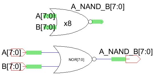
- We already done 2-to-1 gates, now let's make an 8-bit version for them.


- To save time, we will verify the gates at once by putting them all inside a schematic and simulate them.

- The simulation result shows the correct outputs.

- Next part of the lab is the 2-to-1 multiplexer.


- Simulation result: Z=A*S+B*Si. When S=0, B is selected; when S=1, A is selected.

- This circuit can also be used to implement the 1-to-2 DEMUX: use Z as an input and A and B as outputs.

- Now let's verify the schematic.

- The simulation shows the expected outputs for A=Z*S and B=Z*Si.

- Use the 2-to-1 MUX to design an 8-bit 2-to-1 MUX. Use an inverter for Si.


- Simulation shows the correct outputs.

- I also use IRSIM to verify the 8-bit MUX and this simulation also shows the correct outputs.

- Finally,
design the full-adder seen in Fig. 12.20 using 6/2 NMOS and PMOS.
However, I didn't use 6/2 devices for the inverters because I want a
better inverter.

- Once again, verify the schematic.

- The simulations both show the expected outputs.


- We will need to layout the 8-bit adder,
but before that, we have to layout the 1-bit full adder first. I tried
not to use metal 2 because I want to reserve the metal 2 usage for the
8-bit adder so that I can layout the adder a bit easier.

- The full adder passed all DRC, NCC, and Well Checks.

- To implement an 8-bit adder, we can just use the full adder we designed with buses and arrayed icon.

- 8 bit adder IRSIM result:

A
76543210 | B
76543210 | Cin | S
76543210 | Cout |
| 1.00000000=0 | 00000001=1 | 1 | 00000010=2 | 0 |
| 2.01010110=86 | 10100010=162(-94) | 0 | 11111000=248(-8) | 0 |
| 3.01110011=115 | 01000010=66 | 0 | 10110101=181(-75) | 0 |
| 4.10010101=149(-107) | 11000001=193(-63) | 1 | (1)01010111=343(87) | 1 |
| 5.11111111=255(-1) | 11111111=255(-1) | 0 | (1)11111110=510(-2) | 1 |
Note: (1) means overflow with Cout = 1.- Test set 1: Cout = 0, S = 00000010

- Test set 2: Cout = 0, S = 11111000

- Test set 3: Cout = 0, S = 10110101

- Test set 4: Cout = 1, S = 01010111

- Test set 5: Cout = 1, S = 11111110

- Finally
use the full adder to layout the 8-bit adder: drag the full adder to
this layout and make an array of 8, then connect them together. Also
export A[7:0], B[7:0], S[7:0], C0, C8, vdd, and gnd. C0 is the 0-bit
Cin and C8 is the 7th-bit Cout.


- The 8-bit adder passed all DRC, NCC, and Well Checks.


Return to lany3/
Return to EE 421L Labs