Lab 6 - EE 421L
Authored by: Yun Lan
Email: lany3@unlv.nevada.edu
Date: 10/14/13
Lab
description
This
lab is part of the lab project, which is to design a full adder. To
design the full adder, we have to first design the NAND, NOR, and XOR
gates. Of course, we will need inverter(NOT) to implement XOR, use NOT
and NAND to implement AND, and use NOT and NOR to implement OR.
- First, I use 10/2 NMOS and PMOS to design a NAND. Copy the layout I designed before.

- And copy the inverter I designed in lab 5.

- Start drawing the schematic for NAND.


- Next, let's make an icon view for NAND.

- Delete the box, add a half circle, add a small full circle (change the size), and draw the lines.

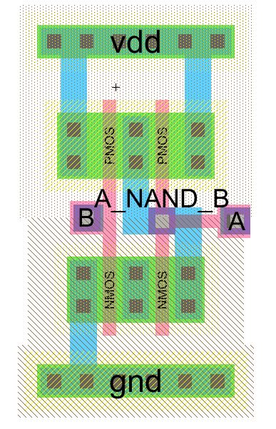
- Before the simulation, let's layout the NAND. Use 10/2 PMOS and NMOS.

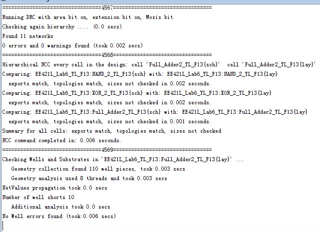
- After the layout is done, do DRC, NCC, and ERC.


- Now we can simulate the NAND gate. Create a new schematic for simulation. Drag the icon into this schematic and enter SPICE code.

- Simulation result: AB=00, out = 1, 01->1, 10->1, 11->0. The results are correct for a NAND gate.


- Simulation
result is same as the schematic because they shared the same netlist.
Therefore I will not include a layout SPICE simulation for other gates.

- Simulation using IRSIM also
has the correct result. Note that you have to change the input values
before the actual test to make the output(s) begin changing.

- After
drawing the input vectors once, I save the vectors so that I can use
this file for other gates (as long as the design has same number of
inputs and outputs and the input/output name is same).

- Layout simulation result same as expected. Note that I use the input vectors file I saved to simulate the layout.

- Similar to the NAND gate, draw the schematic and make an icon for NOR.

- Unlike the NAND gate, we use 20/2 PMOS and 10/2 NMOS to implement the NOR.

- Do DRC, NCC, ERC before the simulations.

- Schematic for NOR gate SPICE simulation.

- Simulation
result: 00->1, 01->0, 10->0, 11->0. The SPICE also shows
the change for the moment a and b changes at the same time (2 us).

- Use the icon and the input vectors file, I get the same result as the SPICE simulation.

- Same result for layout IRSIM simulation.

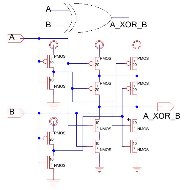
- This
is the last part we need for the full adder and this is the most
complicated gate in this lab. We will need to use 12 transistors, 4 of
them are for A' and B' (inverters).

- The layout of XOR is more time-consuming than NAND and NOR.


- Same as always, simulations.

- Simulation result: 00->0, 01->1, 10->1, 11->0.

- IRSIM simulation using the icon.


- Finally,
we can implement the full adder using the gates we disigned. There are
many ways to implement a full adder, we will implement the full adder
in two ways: 1. use NAND, XOR, NOR, and inverters. 2. use NAND and XOR.
- 1. full adder schematic using NAND and NOT for AND, NOR and NOT for OR.

- Again, simulate the schematic.

- Simulation result: the results are same as the table.
| a | b | cin | | s | cout |
| 0 | 0 | 0 | | 0 | 0 |
| 0 | 0 | 1 | | 1 | 0 |
| 0 | 1 | 0 | | 1 | 0 |
| 0 | 1 | 1 | | 0 | 1 |
| 1 | 0 | 0 | | 1 | 0 |
| 1 | 0 | 1 | | 0 | 1 |
| 1 | 1 | 0 | | 0 | 1 |
| 1 | 1 | 1 | | 1 | 1 |

- However, the IRSIM shows some delays for the outputs.

- 2.
Replace AND with the NAND, the bubbles of the two NANDs go into the
third NAND gate, which is (x' AND y')' -> ((x')' OR (y')') -> (x
OR y). Therefore these three NAND gates have the same functionality as
the NAND, NOR, and NOT combinations in full adder 1. Those two XORs
remain unchanged.

- Simulation schematic and simulation result.


- For
the layout, I drag the NANDs and XORs into the layout and connect the
ports together using metal 2. Although sometimes I will have to use
metal 1 and poly to avoid another metal 2. Connect all vdd (gnd)
together, to form the standard cell frames.


- IRSIM Simulation using the icon and layout of the full adder 2.


Return to lany3/
Return to EE 421L Labs