Lab 3 - EE 421L
Lab description
In this lab, we will design the layout of the 10-bit DAC we designed in Lab 2. For lab2, we used some n-well resistors to implement the DAC and we will layout the n-well resistors in this lab. After the layout, we will replace the n-well resistors by the layout we designed in lab 3. And we will simulate the 10-bit_ADC_DAC to make sure the layout works.
For smaller image size to quickly go through this report, see lab3_custom_sized_imgs.htm.
First, we add a n-well resistoras the following figure shown.
For your infomation, if you don't want to see the black region like those in the following figure, you can hit Window -> Messages Window -> Tile with Edit Window (of course you can make a key binding for this). The message window will automatically fill the black regions.
Open the node properties of the n-well resistor and change the width and length to 12 and 187.5. The sheet resistance of the n-well is 800 ohm/square. Even though 187.5 / 12 = 15.625 which is larger than the ideal L/W ratio 10000/800=12.5, the two nodes of the n-well resistor don't have many resistance. The overall resistance of this n-well is close to 10k.

I use three n-well resistors to implement one of the R2R of the DAC. As the figure shown, the n-well resistors are connected by metal 1. The exporting nodes INPUT, OUTPUT, and B are also connected by metal 1. For measuring the width and length of the resistor, I use the Toggle Measure Distance from the toolbar where the arrow points at in the following figure. The total length of the n-well resistor is 209, but this is not the actual length. The actual length is measured from the N-select to the other N-select, which is 187.5. The width is 12.

The following image shows that the distance from two N-select is shorter than the total length of the n-well resistor.

I use array to make 10 copies to implement the DAC as the figure shown. The inputs (B9 - B0) and output (Vout) and ground are connected by metal 1.

This is the icon for a R2R layout.

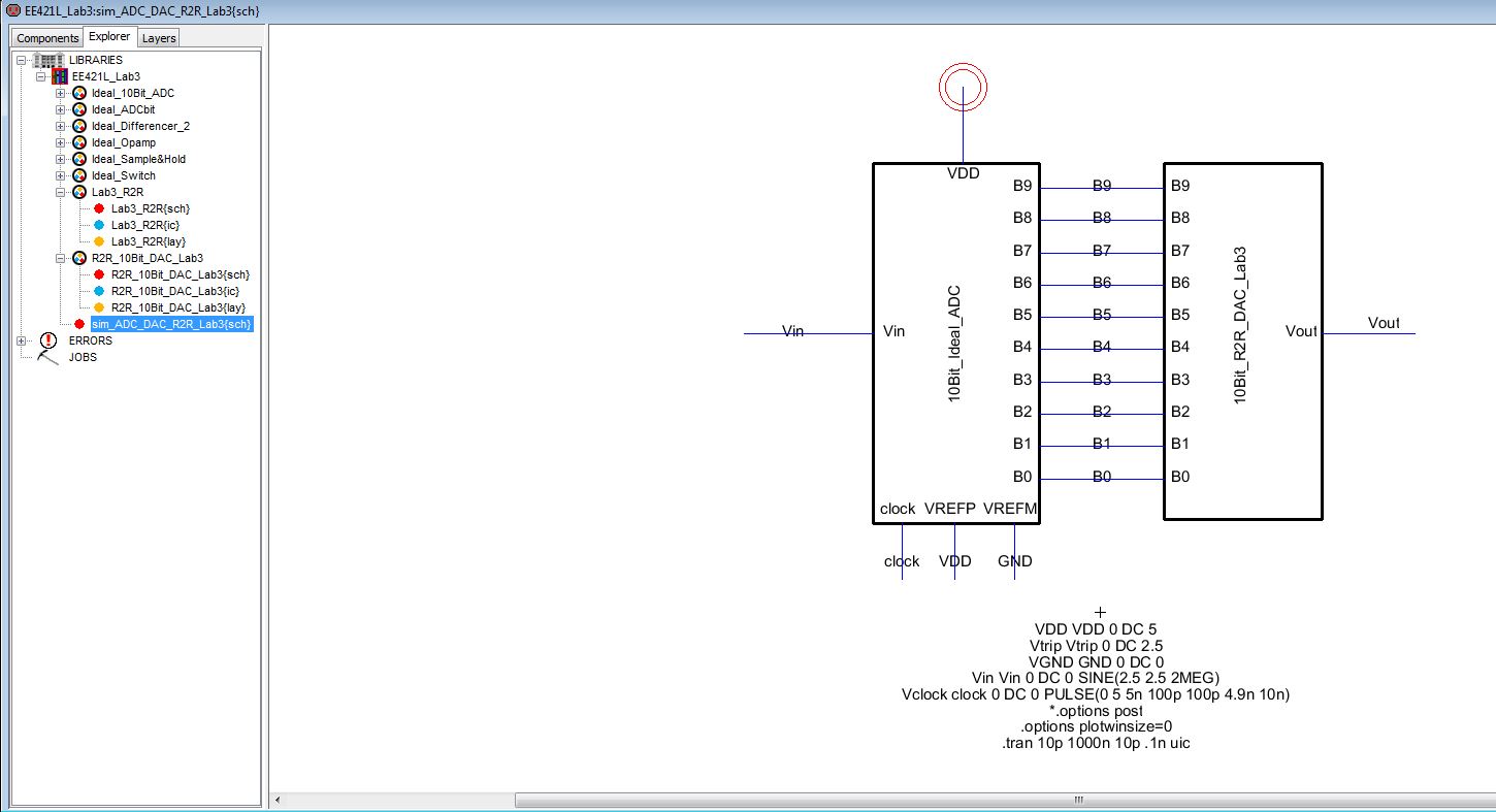
This is how the final DAC schematic looks like. Compared to lab 2, I just replaced the n-well resistors with the n-well resistors I designed.
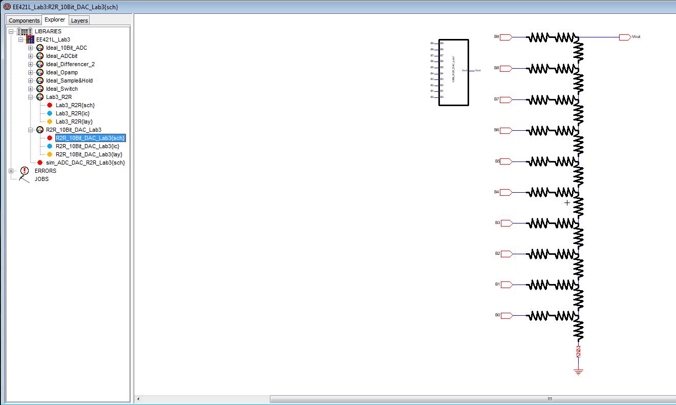
After I replaced the icon for the DAC with the new DAC, the schematic is done.
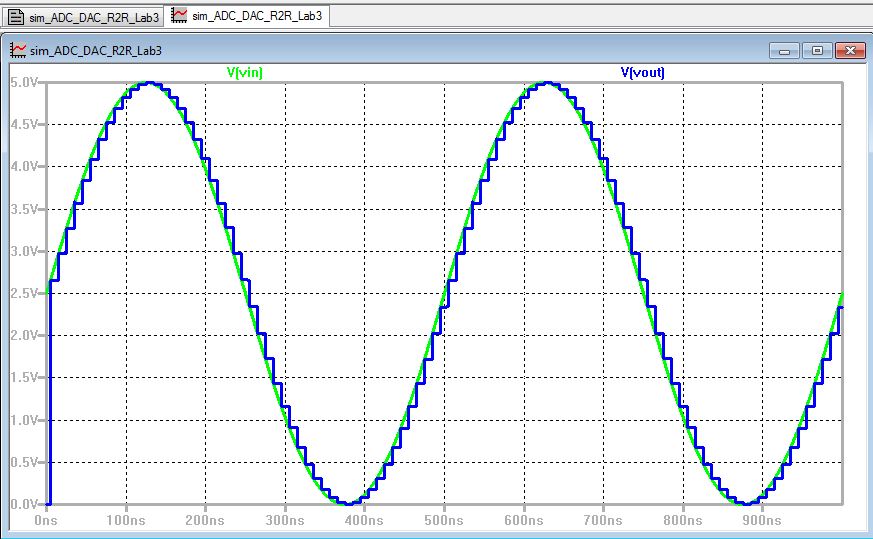
The simulation result is very similar to the simulation in lab 2.
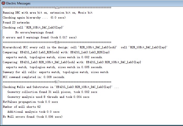
Of course, I did DRC, NCC, and ERC for the design before the simulation. The following image is the results of these three checks.
The lab3 jelib can be found here. If there are errors say that the n-well resistor is not connected to ground, just download the User Preference from here and import. Close the Electric and reopen the library, then do the wells check again.
Here is one of the backups I did: