Lab 2 - EE 421L
Authored by: Yun Lan
Email: lany3@unlv.nevada.edu
Date: 09/12/13
Lab
description
In
this lab, we will be familiar with the ADC (Analog-to-Digital
Converter) and DAC (Digital-to-Analog Converter). The ADC has an input
of the analog signals and converts to discrete time or digital signals.
The conversion is done by sampling the analog signal and holds the
sample until ADC is ready to do the next sampling. For this lab, the
time that ADC holds is depending on the clock (with a certain
frequency). The DAC does the reverse function of
the ADC, DAC converts the digital signal to analog
signal.
Pre-lab
1. Download the lab2 library from here, using the "save link as..." from right-click menu.
Open the "ee421_ecg621_f13" and "lab2" libraries in Electric.
Copy the lab2 library to the ee421_ecg621_f13 library by:
Click Cell->Cross-Library Copy...
Select the "sim_ADC_DAC{sch}" from the lab2
Check the Copy subcells and Copy all related views
(these steps will copy all other files that is related to the file you
select)
Hit << Copy (Make sure you are copying to the ee421_ecg621_f13 library)

2. Save the library and close the lab2 library after copying.

3. After saving, do a regular backup to back up the work when needed.

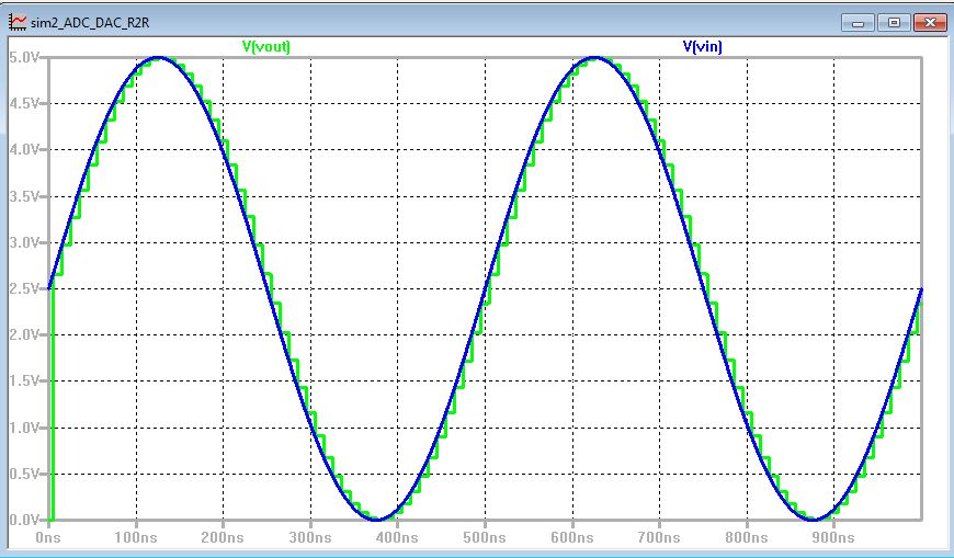
4. Run the simulation and view the waveforms of V(vin) and V(vout).
5. V(vin) shows a sine wave and V(vout) shows the discrete time.

6. V(vout)
only changes at the rising edge of the clock, which means the ADC
samples V(vin) at the rising edge of the clock and holds until the next
rising edge.

7. V(b4) is part of the output of the ADC, the figures below indicates that the
value of V(b4) will only change when the rising edge of the clock
occurs, if there is no change is required, the value of V(b4) will be
hold until there is change to be made.


8.
The digital signal can be represented by binary, which the least
significant bit (LSB) is the rightmost bit in the digital code. The
smallest possible change represents the LSB in the analog output
voltage of the DAC. 1 LSB =V_ref / 2^N. For a 10-bit DAC and with a reference voltage 5V, 1 LSB will be 5/2^10=4.88mV.
Lab Report
- The design of a 10-bit DAC using an n-well R of 10k
- We
are using n-well resistors to implement a 10-bit DAC similar to Fig.
30.14 below, in the CMOS book. However, in lab 2, we will use the ADC
in the lab2 library instead of using the switches as inputs.

- The
two figures below show the schematic of the 10-bit DAC. I placed two
10k n-well resistors in series to implement the 2R resistor.


- After replacing the 10Bit_Ideal_DAC using the 10Bit_R2R_DAC
schematic, there were many errors showed up when I did the Check
Hierarchically. Most of them are the connection errors between the ADC
and DAC. Using the Cleanup Pins Everywhere from Edit -> Cleanup Cell
actually removed most of the extra pins.

- The
output resistance of the DAC is the total resistance at the node Vout =
((20k || 20k at the node near to the B0) + 10k) || 20k at the node near
to the B1 + ...(similar to the steps above). Finally, at the node Vout,
R_out = 20k || (10k + 10k (overall R from B8 to B0)) = 10k = R.
- The delay of the DAC with a 10pF is 0.7RC = 0.7 * 10k * 10p = 70 ns.


- Click Cell -> New Cell... to create a new icon.


- Select Component -> Export -> Bus to create the ports


- There is also an easy way to make an icon view: go to the schematic of R2R_DAC and View -> Make Icon View.


- When the icon is done, I replaced the icon copied from lab2 library with the new icon I designed.

- Simulations
- The simulation below shows a same waveform as the waveform in pre-lab.

- When
the DAC drives a 10k load, the output is half of the input because the
10k load only get half of the input voltage (Vin * 10k / (10K + 10K).


- When the DAC drives a C, the output has a magnitude change and phase shift because the DAC itself has an output resistance 10k.


- When
the DAC drives a R parallel with a C, the output is similar to the DAC
with a C but the output of DAC with R/C is smaller because the load R
reduces the output voltage.


- If
the resistance of the switches is closed to R, then the output
resistance will be higher. For example, if R_switch = 10K, then (10K +
20K) * 20K (assumed, total R from B0-B8) / (50K) = 12K > R_before =
10K.
Return to lany3/
Return to EE 421L Labs