Lab 2 -
EE
421L
Design of a 10-bit Digital-to-Analog Converter
(DAC)
Authored
by Min Lan
LANM2@UNLV.NEVADA.EDU
09/13/2013
Electric library: ML_ee421L_f13_lab2.jelib
Note: Click on image
to see original image in new tab/window.
Lab
description
We will use n-well resistors to implement a 10-bit DAC.
The design would be based on an simpler DAC below, from our textbook:

Without
explaining how this DAC work, the output would be multiple of 1 LSB
voltage
In
the above circuit, 1 LSB = VDD/32. For example, when only b4 is tied to
VDD and all
other
bits are tied to the ground, the output voltage will be 1/2 of VDD.
Similarly,
when only b3 is tied to VDD, and all other bits are tied to the ground,
the
output
voltage will be about 1/4 of VDD.
Using
principle of superposition, each bit contributes to the output voltage
by about
2-N
of VDD voltage.
When
all bits are tied to VDD, then the output voltage will be equal to VDD.
If
we increase the number of bits, then we can generate finer voltage:
1/64, 1/128, or
1/256
of VDD.
In
general the voltage can be estimated by number represent by b4b3b2b1b0
in binary
multiplied
by 1 LSB voltage.
For
b4b3b2b1b0 = 010112 = 1110,
Vout ≈ 11xLSB = 0.344 VDD.
Output
Resistance of DAC:
To
determine the output resistance, look at each black dotted junctions:
Starting
with the lowest junction/node, the resistance looking down is 2R,
which
is connected in parallel with the horizontal 2R resistor to the left
of
the node. These two 2R resistors in parallel have equivalent resistance
of
R, and when added to the R resistor (in series) above the node, the
total
resistance looking down the 2nd node (count from the bottom)
is
2R.
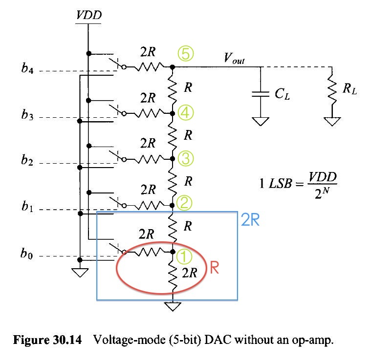
Now
replace the subcircuit below the node with a 2R resistor, we obtain
the
exact same circuit as the 2nd node. Repeating the procedure we
can
conclude that the resistance looking down every black dotted node
is
2R.
In
the end, we will have only two 2R resistors connected in parallel
looking
at the Vout node. The output resistance is 2R||2R = R.
The
output resistance of a 10-bit R2R DAC is the same as the 5-bit
DAC.
10-bit
DAC
Using
the 5-bit DAC as a model, we can build a 10-bit DAC by placing
5
more vertical R resistors below node 1, each separated by a new
node,
and then connect to left of each new node a 2R resistor and
then
a switch (bit input).
Lastly,
connect the only vertical 2R resistor between the lowest node
and
the ground.

Create
an Icon for the DAC
First,
with the schematic window open, under menu View, select Make Icon View.
Select
the generated icon and press Control-D to edit the icon.
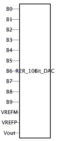
Adjust
the size (to 10x22) to match that of the ADC in used in cell
sim_ADC_DAC. Rotate
the
text "R2R_10Bit_DAC, move Vout to the right, reference voltages to the
bottom, and finally reposition the inputs. Add text annotation to every
pins inside the box.
Without
deleting the pin, wires can be re-drawn and sized so that they touch
the box.
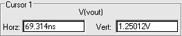
Delay,
driving a load
Make
a duplicate of the cell sim_ADC_DAC, remove everything except the spice
code.
Drag
the created icon R2R_10Bit_DAC{ic} into the schematic window.
Ground
all DAC inputs except B9. Connect B9 to a pulse source (0 to VDD), and
connect
a
10p capacitor to Vout.

The
delay is expected to 0.7RC = 0.7 * 10kΩ * 10pF = 70ns.

The
simulation result gives 69.3 ns, which is close.
Simulation
and Verification
The
ideal DAC is replaced with designed DAC.

and
the simulation produces the same output.

Driving
a load with DAC
Driving
a resistor:
The
resistive load creates a voltage divider, the output voltage is equal
to Vin*RL/(R+RL).
When
RL = 10k = R, the output voltage is half of the
input voltage.

Driving
a capacitor:
The
capacitor causes the phase of the output voltage to shift in AC as the
frequency varies; and with
the
internal output, the amplitude diminishes as well.

Driving
a resistor and a capacitor:
The
load resistor added to the circuit above lower the amplitude further.

In
real circuit, if the resistance of the switches is not small, the
output resistance without load
will
increase, which contributes to greater output voltage in the voltage
divider.
Return to EE 421 Labs