The final project for this lab will be the design from schematic to layout of an ALU capable of 4 operations, Logic AND
Logic OR, Arithmetic Add, and Arithmetic Subtract, the operands for this ALU will be 8 bits in length A[7:0] and B[7:0].
The first step of this design will be the schematic, which can be seen below.
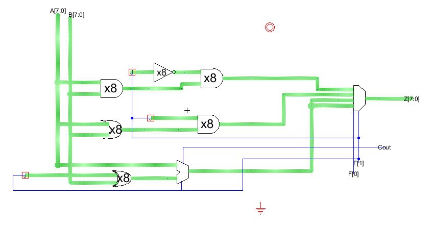
Before moving on some of these components in the ALU require a brief explanation, as they were not constructed before
this project.
Firstly, a 4 to 1 DeMux/Mux was required for the selection feature of the ALU, this was done using 3 single DeMux/Mux's
The first selection input is used to pick from either the top inputs or the bottom inputs of the first 2 DeMux/Mux's and the
second selection input was used to select from the two remaining inputs that were passed through the first DeMux/Mux's.
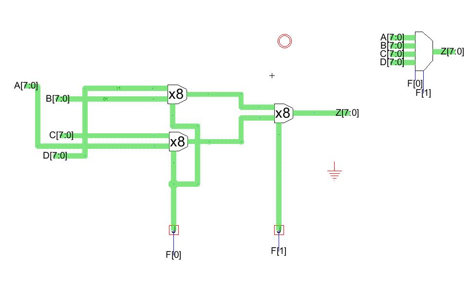
By taking this design and using multipliers an 8 bit, 4 to 1 DeMux/Mux was created (seen below).
Another thing used in this design that may be different from others is the use of an XOR gate on the input of the B bus. This
gate is used as a sort of switched inverter, seeing as the XOR will invert an input when a logic "1" is applied to the other
this allows us to choose to invert the B input when we want subtraction to be performed. This selection pin is also tied to Cin
allowing us to represent 2's complement subtraction. This method allows us to use only one Full Adder whose output is tied
to both Arithmetic DeMux/Mux inputs.
One last thing to mention is the And gates tied to both the OR and AND outputs, this is placed here to gate the outputs so that they
only output if they are selected by the F pins.
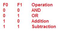
The operations that will be carried out follow this truth table, this setup was very convenient as a 0 in the F0 means Logic operation,
and a 1 means an Arithmetic, we can then tie the F1 pin to the Cin and XOR table.
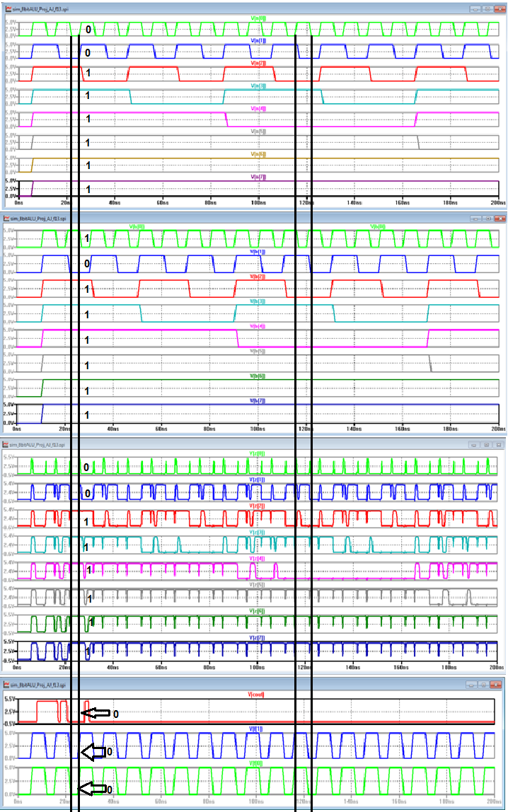
Below is the first simulation performed on this schematic using LTspice, it shows that when the AND
operation is selected the outputs behave accordingly. However the next highlighted point should be
a subtraction, as it has a 1 and 1 selected on the F pin respectively, we do not recieve a clean signal
some of this can be attributed to offsets on the signals but this is a problem that must be attended to.
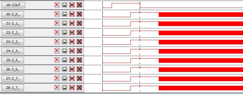
Using logic software specialized for logic design, this error will be checked.
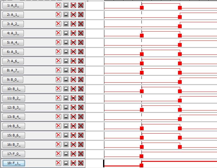
Here the inputs have been set to the values we had before.
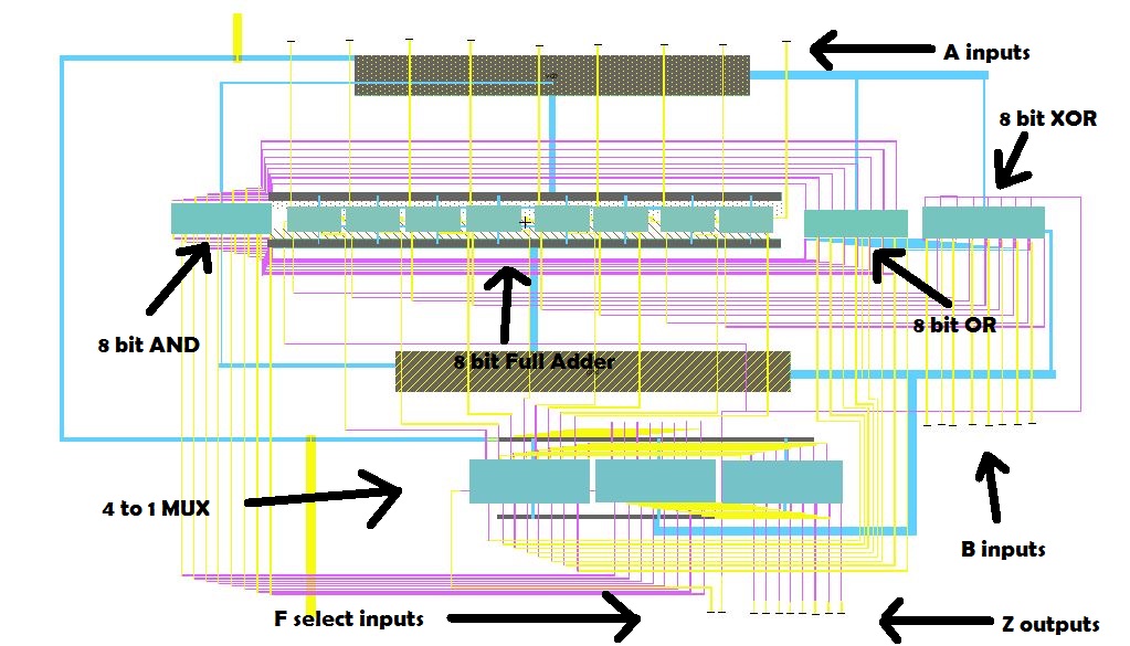
The final step of this project is to layout the ALU.
In order to do this some previous lab's layouts had to be recruited and adjusted to be placed into this final design.
The full adder, because it is the heart of this ALU, was the first to be placed into the layout. To form the correct
8 bit full adder, the single bit adder was cascaded 8 times with each Cout fed into the Cin of the next full adder.
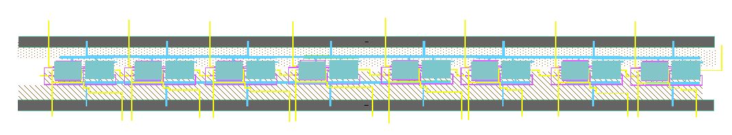
The next step will be to put together an 8 bit 4 to 1 MUX constructed from three 2 to 1 MUXs.
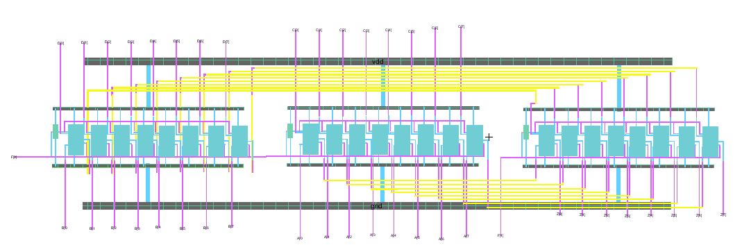
Once this is finished I simply placed AND, OR, and XOR gates (8 bit gates), connected the gates together correctly, set the correct input
and output exports and DRC, ERC and LVS the layout to make sure it matches the schematic.