Lab 6 - ECE 421L
Authored
by Aran Johnson
Email: john1701@unlv.nevada.edu
October 11th, 2013
Lab
description:
In this lab experiment we will:
-Create schematics for a 2-input NAND gate, NOR gate, XOR gate, and a full adder
-Make icons for each of these schematics
-Construct layouts for each of these circuits
-Use IRSIM and LTspice to simulate the logic function of these gates
Prelab work:
-the prelab for this lab was to work through Tutorial 4 and the Electric video on building NOR gates
-as usual backup all previous work
Lab steps:
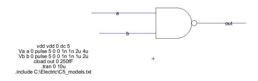
NAND GATE:
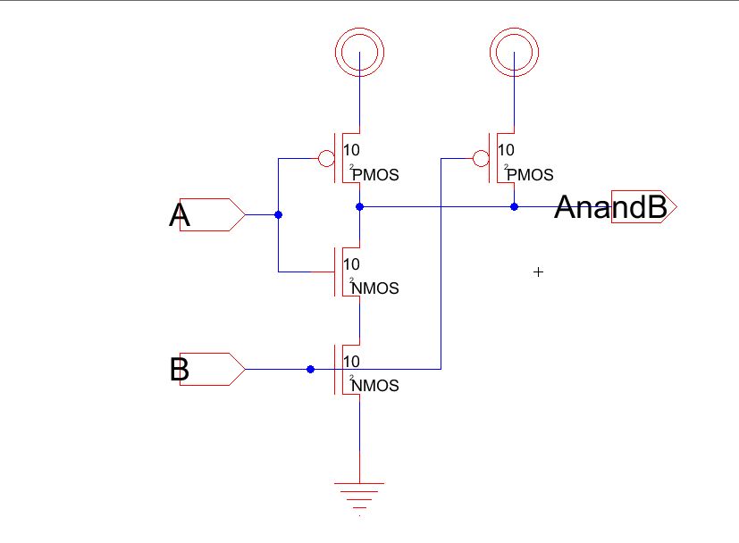
We will begin by drafting the schematic of a 2-input NAND gate in Electric. We will size all of our MOSFETS
in this schematic to be of size 10/2, with a width of 10 and a length of 2.
Each of our schematics, icons, and layouts will be named (gate type)_(your name initials)_(semester and year)
like how I have named my NAND gate NAND_2_AJ_f13.
As we did before we set the spice model of each transistor to PMOS and NMOS so that
we can have a correct model for each transistor. We navigate to Tools->Simulation(Spice)
->Set Spice Model... for each transistor.
From here we can create an icon that will match the logic gate. We move to
View->Make Icon View, and from here we will edit the symbol to match a NAND gate.
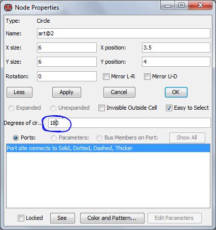
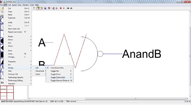
First we need to create a semi circle for half of the gate. We first select a circle in the
components tab and set the degrees to 180 so we only get half of the circle.
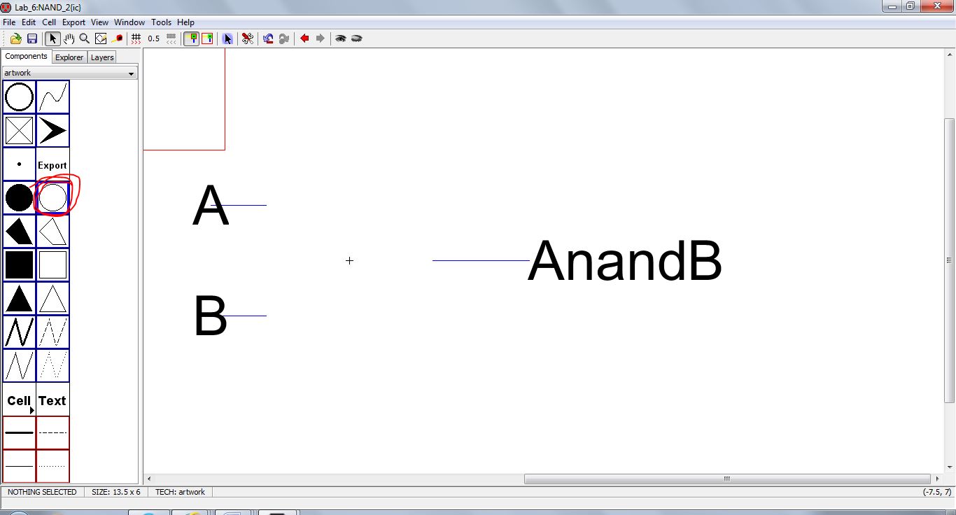
Then we can drop a line segment in and select it to edit the outline as seen below to create the second half
of the icon.
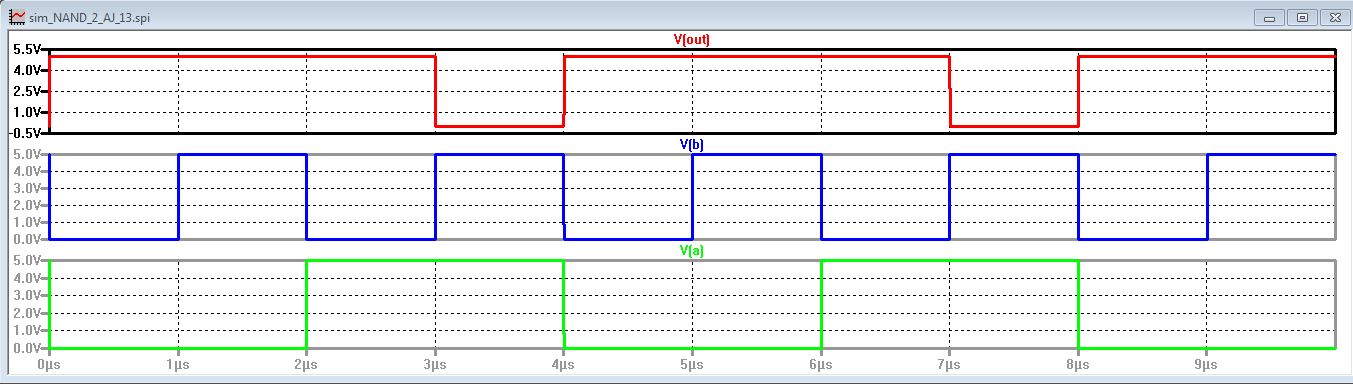
We now have an icon view that we can use to simulate with. So we create a cell titled sim_NAND.....
The truth table for the NAND gate is
This is demonstrated in the results below, only when both the inputs are high, is the output low.
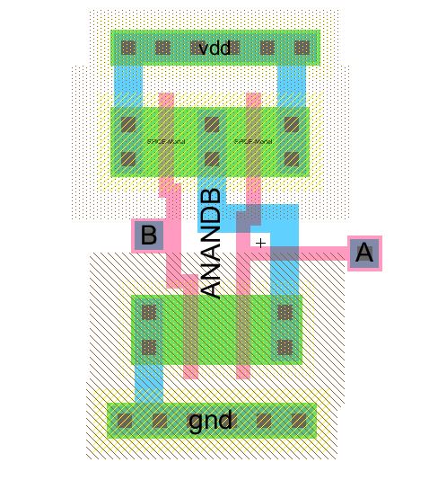
We will now layout the NAND gate, we start with a single PMOS and NMOS transistor.
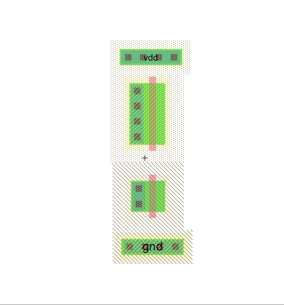
We then add another PMOS and NMOS transistors, and make the corresponding connections.
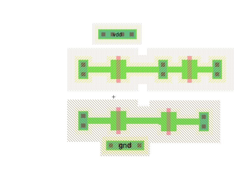
Then we add a few more connections and now have the whole thing connected, making sure that our
inputs (A,B), outputs (ANANDB) and our Vdd and ground are on metal 1.
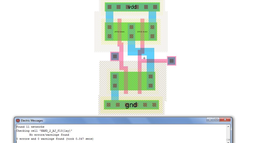
We then DRC our layout for a rule check to make sure everything falls in line with our process rules. After that we run a well check,
and an LVS to ensure that our schematic matches our layout.
NOR GATE:
We will now move onto a two-input NOR gate following the same procedure, except in this schematic we will use
20/2 PMOS transistors and 10/2 NMOS transistors.
Our name for the gate schematic, icon and layout will follow the same format as the NAND gate, I named mine
NOR_2_AJ_f13.
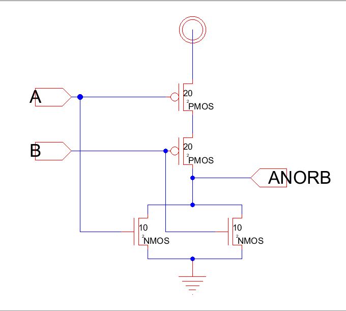
As you can see, this gate is constructed much like the NAND gate except for the use of 20/2
PMOS transistors.
We export the A and B inputs, as well as the ANORB output, but not the vdd or ground pins.
From here we will create an icon for simpler use later in the lab, this icon, like the NAND gate,
must be easily identifiable as a NOR gate.

This
icon will suffice for our simulation needs, and later implementation
needs. Next we must create a sim schematic for simulating
this NOR gate. We will alternate the inputs from 0 to 5V in differing periods to see each possible logic input.
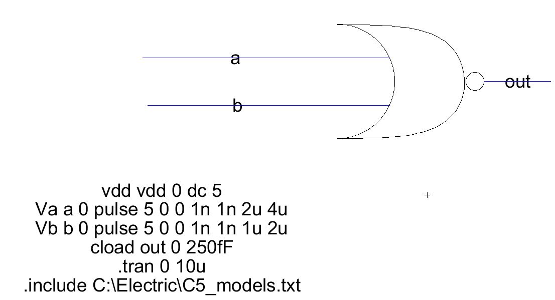
If we succeed we should see something that will match this truth table.
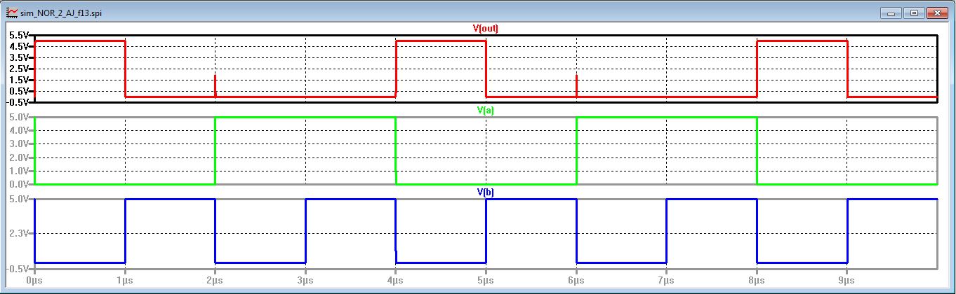
As
you can see we only achieve a value of "1" when both inputs are at 0 V
which follows the truth table. The small peaks can
most likely be attributed to current changes across a capacitor.
We
can now move onto our layout of the NOR gate. In this layout
notice that the PMOS transistors are now twice the width
of
the NMOS transistors, instead of them being the same size like they
were in the NAND gate. Also we make sure to keep
the exports on metal 1.
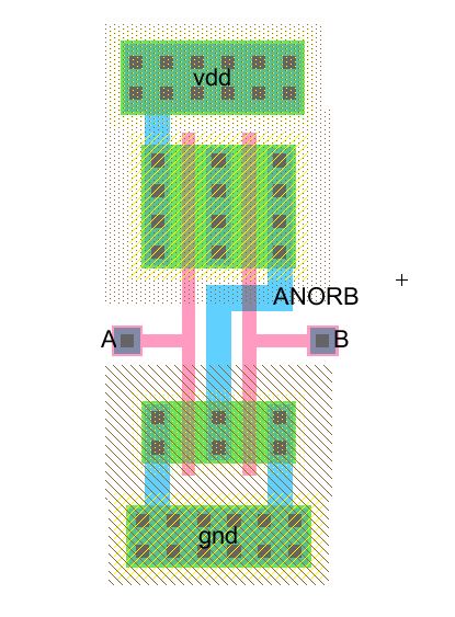
Once we DRC, ERC, and LVS the layout we can now move onto the next schematic.
XOR Gate:
We will now move to an XOR gate schematic, icon, and layout. Similarly to the NOR gate
we will draft this schematic using 20/2 PMOS and 10/2 NMOS transistors.
This gate requires the use of inverters, so we will recruit icons from Lab 5 of our inverters to
draft our XOR schematic. We open the Lab 5.jelib and drag the icon into our schematic and then
connect the rest of the MOSFETS together.
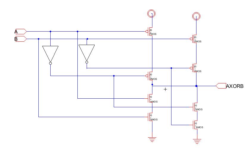
An icon will be very handy for the XOR gate because of its greater complexity when compared to the NAND and
NOR gates.

We can now simulate our XOR circuit to see if it matches with the expected truth table below.
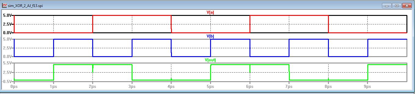
The
simulation gives us the expected results, when the two inputs match
eachother, the output is a low voltage, and when the two inputs are
opposites the output goes to high.We can grab the layouts of the inverter and use them in our layout for the XOR.
Because of spacing the two vdd's were forced to be shorted using the metal 2 layer, but
besides this all of the exports and gnd are kept to the metal 1 layer.
The circuit DRC's, ERC's and NCC's, allowing us to move on to another circuit.
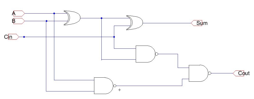
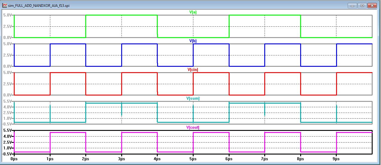
Full Adder:
When
we draft the schematic of the full adder we can use the previously
created icons from the inverter, NAND, NOR and XOR gates.
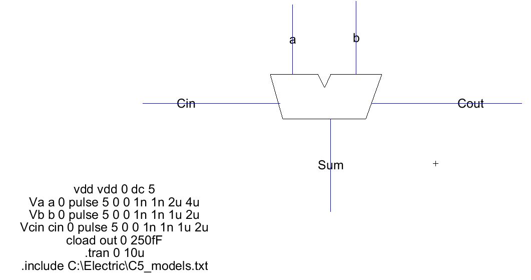
 We can now make an icon for the full adder to simplify simulation as we did with the previous logic gates.
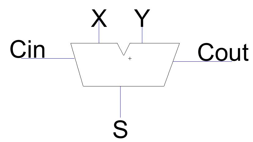
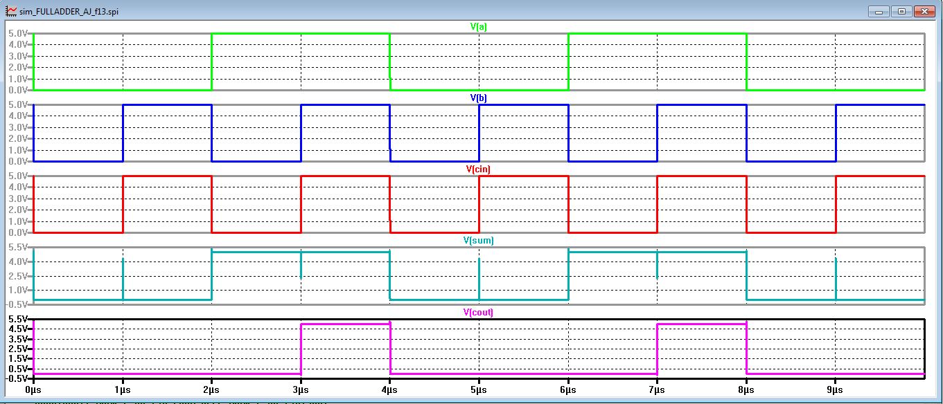
We
will now use this icon to simulate our full adder and test to see
whether its output matches that of the truth table below.
| A | B | Cin | Sum | Cout |
| 0 | 0 | 0 | 0 | 0 |
| 0 | 0 | 1 | 1 | 0 |
| 0 | 1 | 0 | 1 | 0 |
| 0 | 1 | 1 | 0 | 1 |
| 1 | 0 | 0 | 1 | 0 |
| 1 | 0 | 1 | 0 | 1 |
| 1 | 1 | 0 | 0 | 1 |
| 1 | 1 | 1 | 1 | 1 |
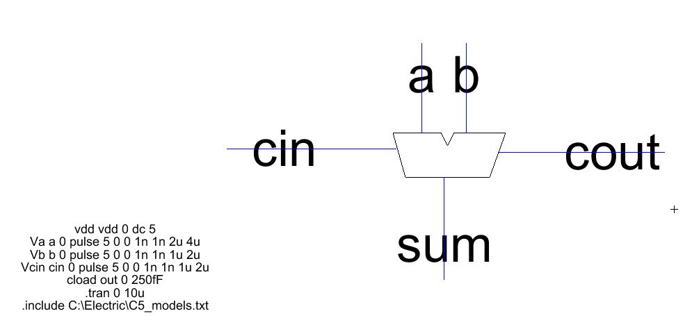
We use our icon and set up spice code to simulate our circuit to have input of each possible value.
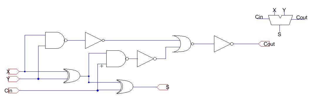
Next we explore another form of full adder, using three NAND gates and two XOR gates.
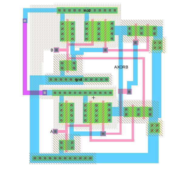
We
will now create a layout of this full adder, making sure to lay them
out end to end so that ground and vdd are routed, and place the output
and input pins on the metal 2 layer.
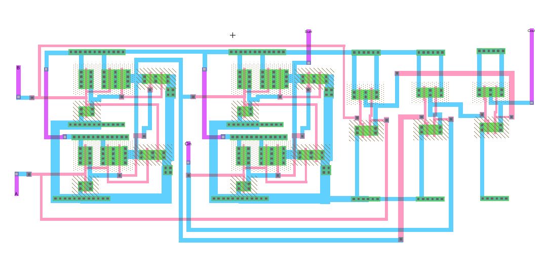
Once we finish our layout we can, again, create an icon for our schematic to make simulations more simple.
We
vary the inputs to achieve different binary values to see if they work
with the truth table we used for our previous full adder.
After a look, we can see that our truth table matches the simulation. .jelib
Return