
Lab 4 - ECE 421L
Prelab work:
- work through Tutorial 2 to gain an understanding of how to both construct
the nmos and pmos schematic and layout the transistors.
-backup all previous work done
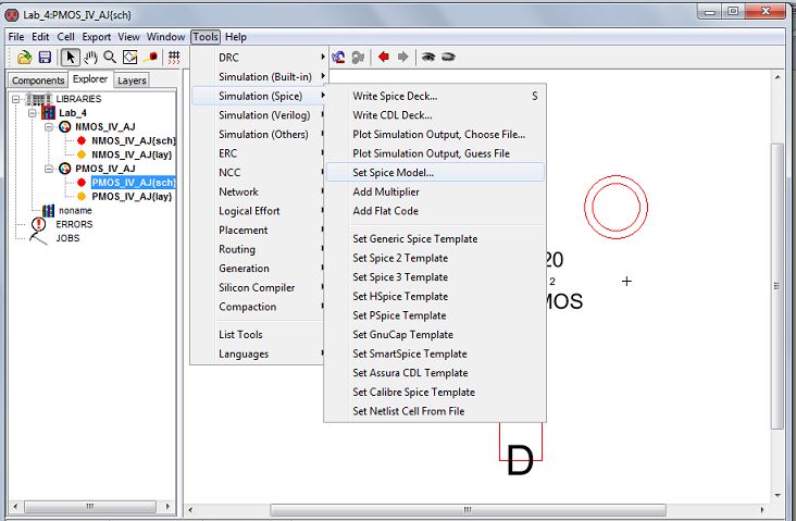
In order to simulate these transistors' IV characteristics we must set the models of these MOSFETS to match
there names, to do this we will navigate to Tools->Simulation(Spice)->Set Spice Model and from here name the
spice models NMOS and PMOS. This will link the models to the saved models in C5 Models.txt, copy it here for
use later in the simulations.
Now, to simulate the IV characeristics of these transistors we will create two more cells dedicated to just
simulating them titled sim_NMOS/PMOS_IV.
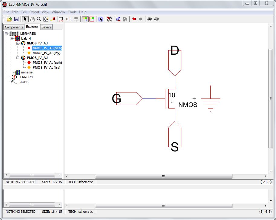
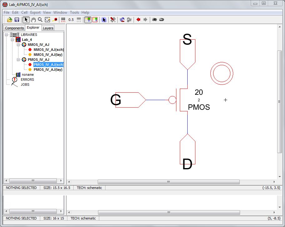
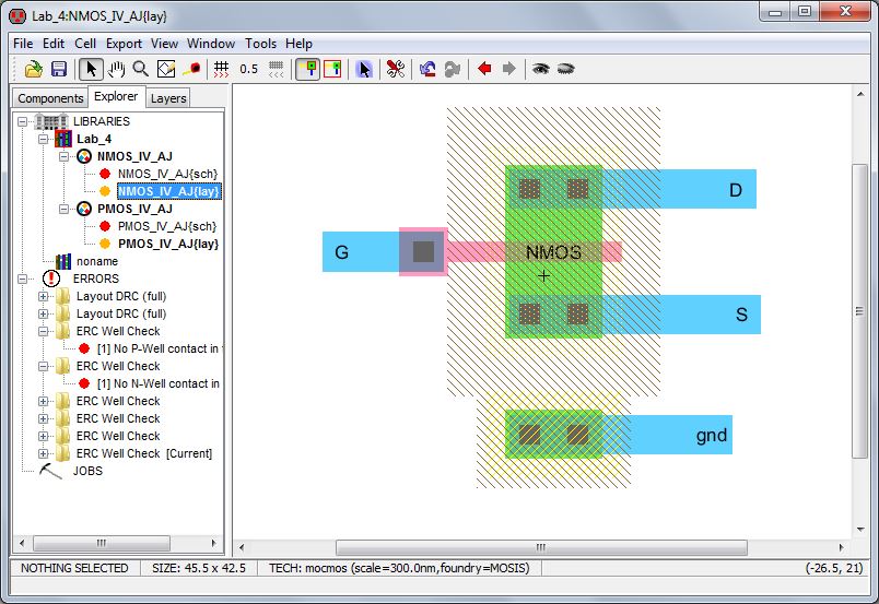
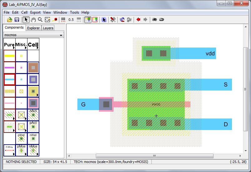
Before we actually simulate these circuits we will lay them out in Electric. We start new layouts under the
same title as the schematics. Then navigate to the components menu and choose the nmos and pmos transistors.
We then connect the drain and source to n-active to metal 1 contacts for the NMOS transistor or p-active to metal 1
contacts for the PMOS transistor. Then we need to connect the Gate, we do this by using a poly to metal 1 contact, for
both transistors. Finally we will connect ground or vdd depending on the transistor, for the NMOS we will connect a
p-well to metal 1 contact and set the export to gnd so that the p substrate will act as our ground. In the PMOS transitor
we will place an n-well to metal 1 contact and set the export to vdd so that our n-well will now stand as our VDD. We now
DRC and ERC our layout to check for any errors and fix any sort of errors that occur.
![]()
![]()
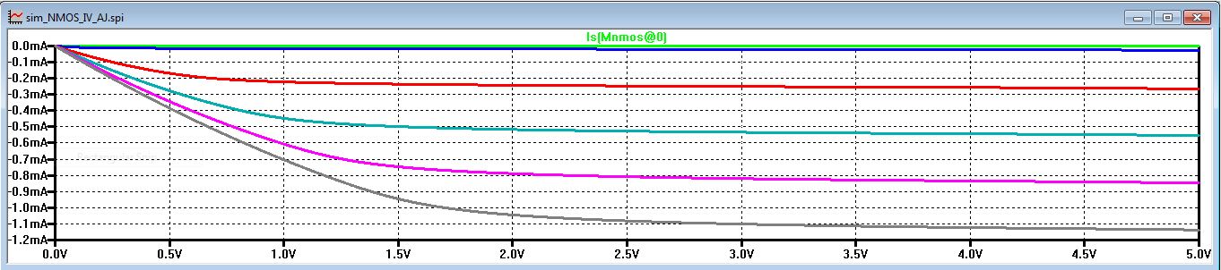
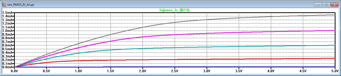
Each one of the curves represents a different value of the Gate Voltage ranging from either 0-5V or -5-0V