Lab 3 - ECE 421L
Authored
by Aran Johnson
Email: john1701@unlv.nevada.edu
September 20th, 2013
Lab
description:
This lab experiment will:
-focus on the layout of a 10-bit DAC using n-well resistors, which was previously designed in lab 2.
-help to reinforce knowledge of creating and using icons.
Lab steps:
First
we must lay out an n-well resistor, not just a regular resistor, and
scale its size to suit our necessary resistance requirement.
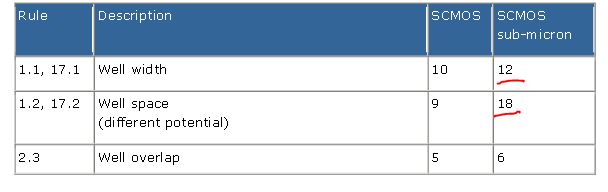
Here
we can see that the well width must be at least 12 lambda, and the
spacing must be at least 18 lambda, in the C5 CMOS process.
We
will design our circuit around 10K resistors, and after a quick look we
can find that the square resistance of our process in the n-well
will
be approximately be 800 ohms/square, meaning that we will need a width
and length with a ratio of 1:12.5, in order to get as close to
the minimum as we can we use 15 and 187.5 as our width and length, respectively.
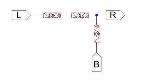
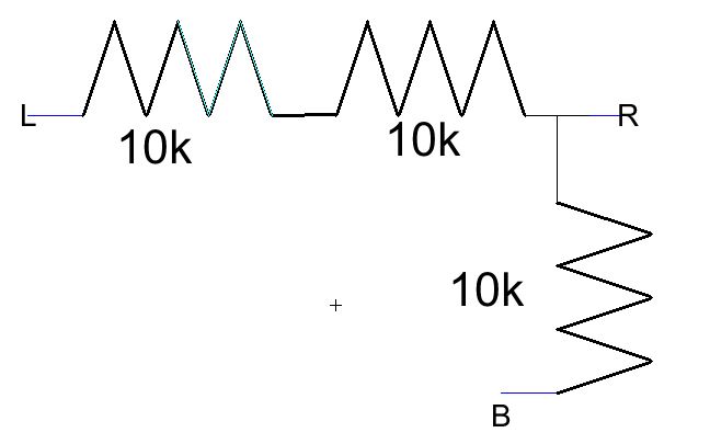
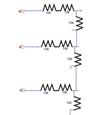
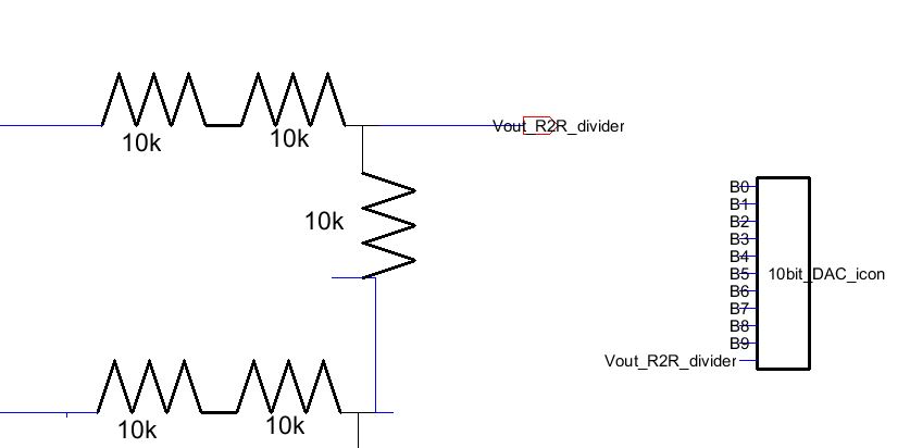
Now
we will use three of these resistors to create one of our bit
converters for our final DAC. We will use an L node for the
incoming bit,
an R for the outgoing signal, and a B node for connecting to the other bits.
We can now creates an icon for this schematic to implement into our design by navigating to View->Make Icon View.
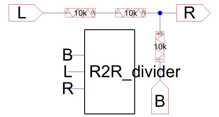
We now have an icon to work into our next few steps of the schematic.
Now, by moving to the icon view itself, and by using the artwork in the explorer box, we can change the icon into something
that will better represent our subcircuit.
Once we finish with our icon view, we can now cascade this icon we have constructed and begin working on the final design of our
DAC. We will revisit this setup later, but now we will move to the layout of the circuit.
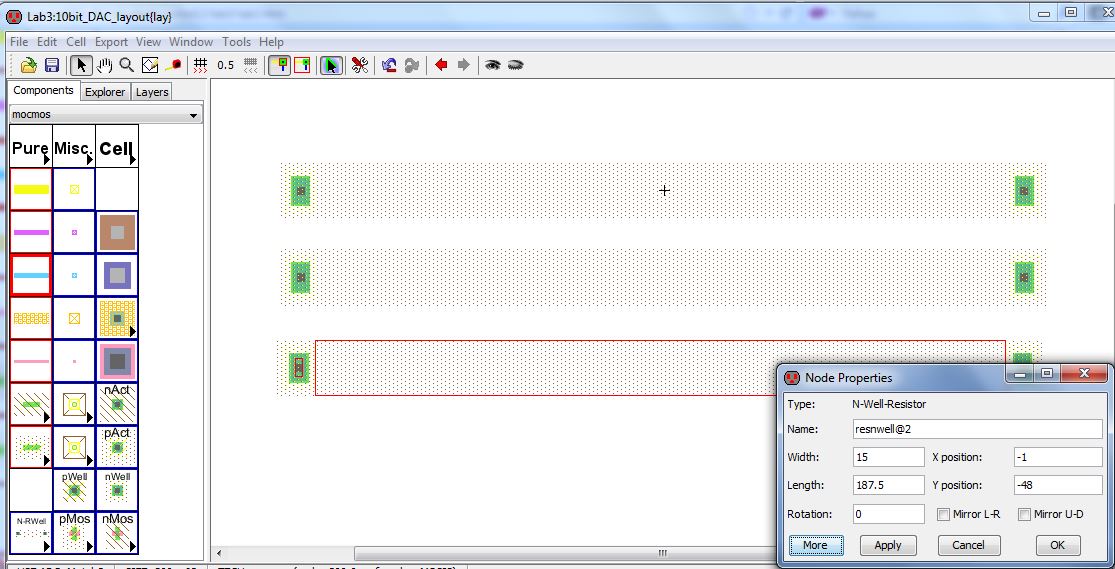
We
select an n-well resistor by navigating to the arrow in the box in the
bottom left corner of the components box, and knowing
that the width must be 15 and the length must be 187.5 we adjust these values accordingly.
One
thing that must be pointed out is how the measurements work. As
you can see, the lengths of the resistor are taken from inside the
contact
points because the current obviously will not travel through the ends
of the n-well. The width however is taken from across the
resistor.
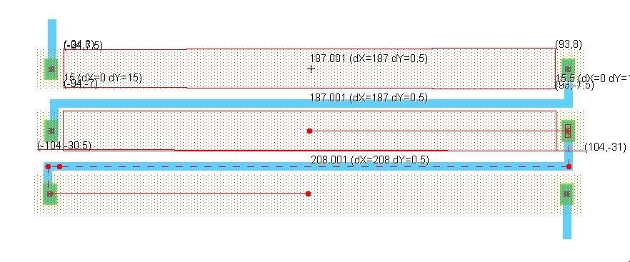
We
must also make sure that the space between the resistors is not less
than 18 lambda so that the circuit stays within the boundaries
of our CMOS process.
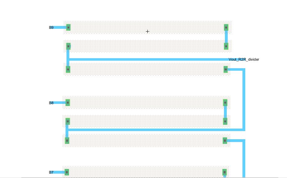
Now we can set exports for each bit and the output of the whole DAC, as well as connecting each of the resistors.
Now
we can move back to our original schematic, we can put in an output pin
calling it R2R_divider. From there we can
again create an icon for our final circuit for use in our final simulation.
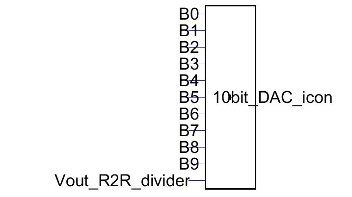
Here is a more clear image of our icon for our 10 bit DAC.
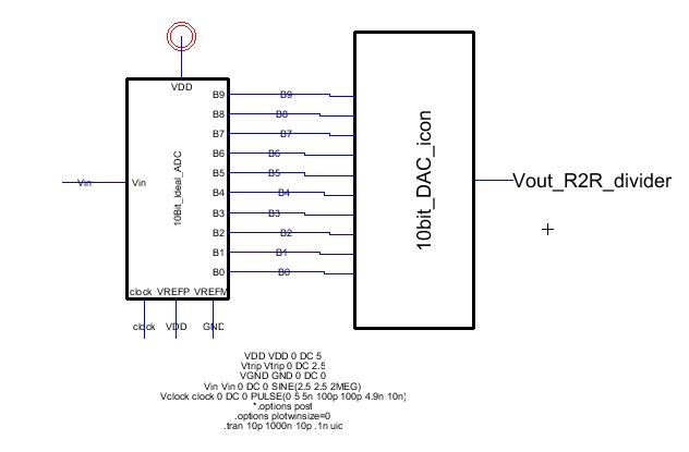
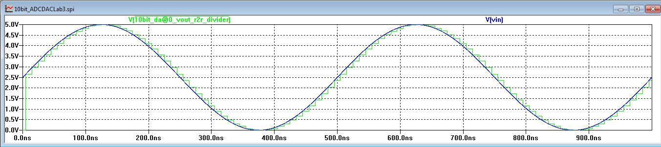
We can now take the original ADC/DAC circuit and remove the DAC in order to simulate our DAC to see if it
matches the original simulation.
Jelib file
Return