Lab 2 - ECE 421L
to illustrate your understanding of the ADC and DAC
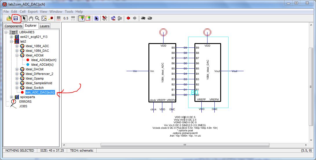
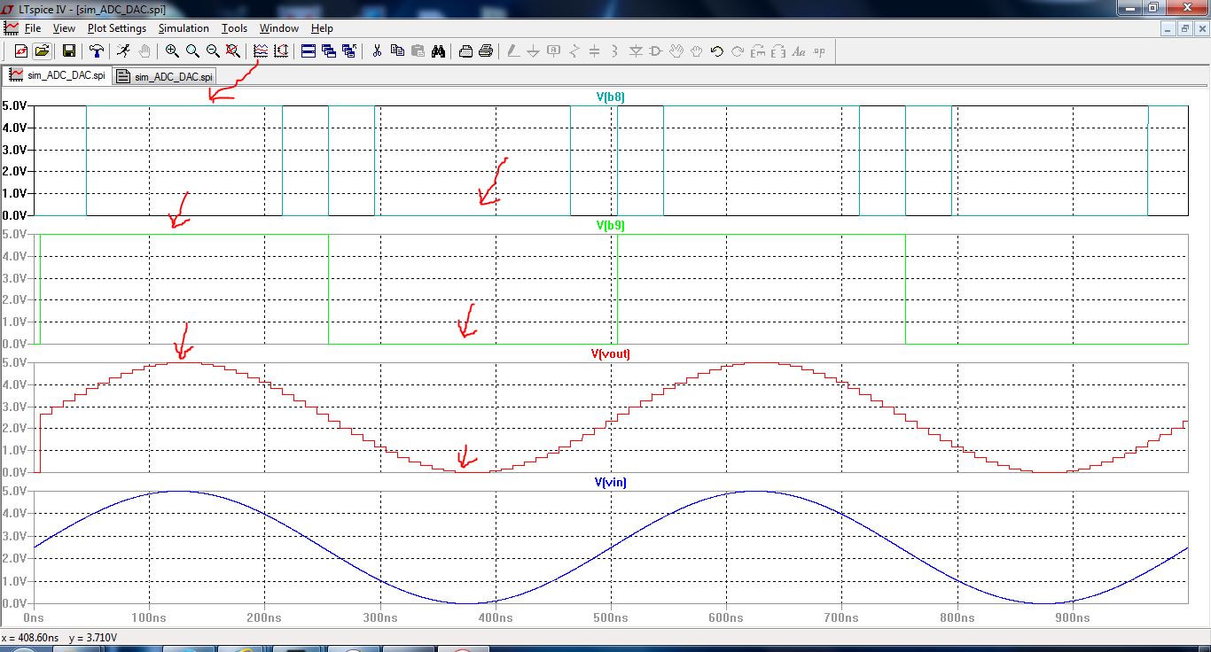
on the ADC's input to see a change in the digital code B[9:0]) of the converter.
Use simulations to support your understanding.
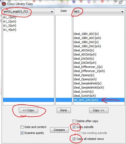
After this task was completed we navigated to "Done," and needed to save our current course/lab jelib.
Then, after backing up the work we have completed thus far, we ran the simulation using 'S' as a keybinding, or by selecting
"Write Spice Deck..."
Results differing from prelab:
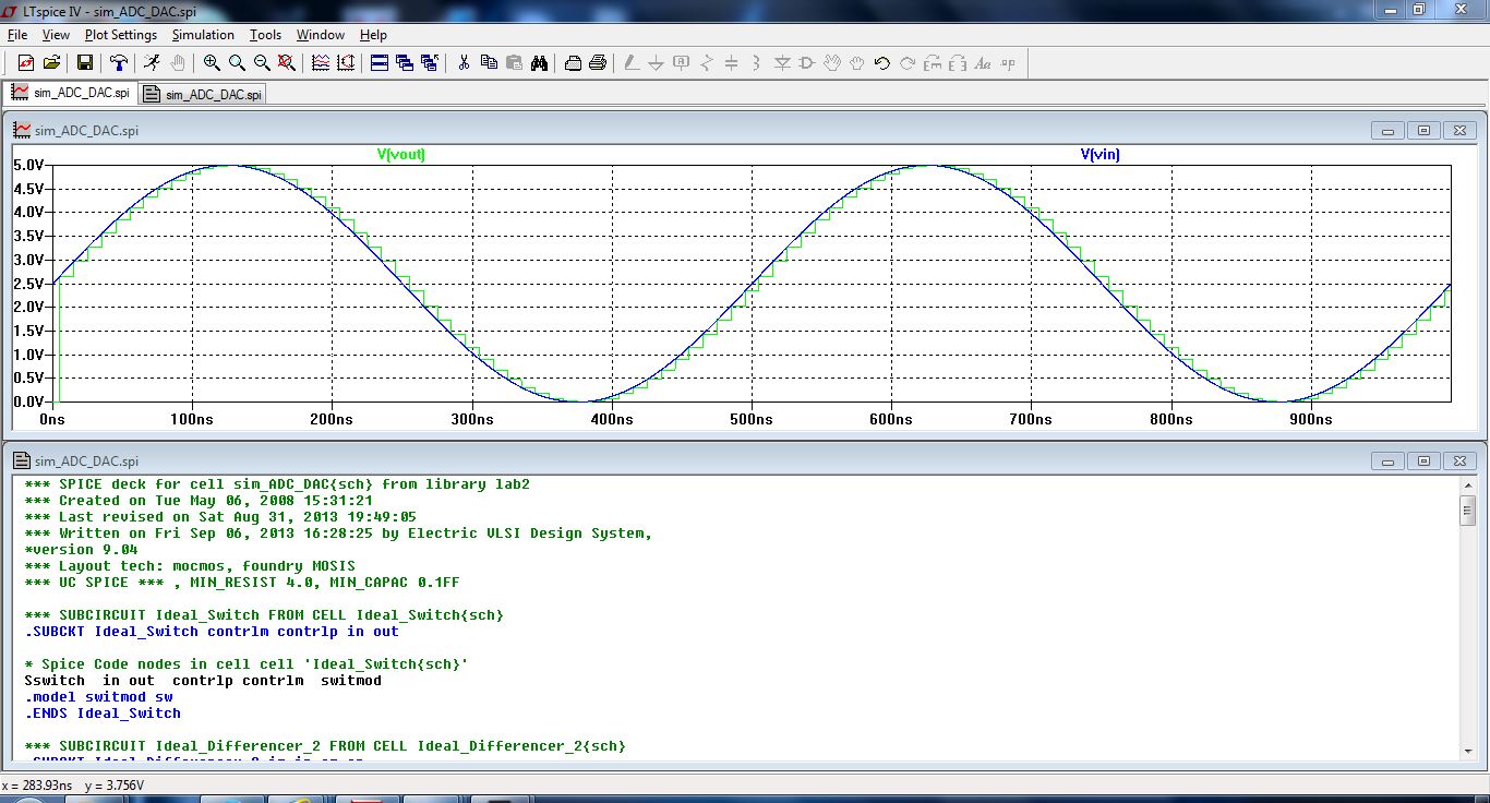
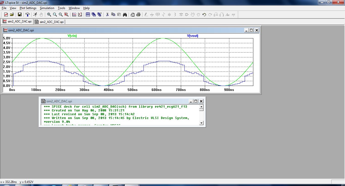
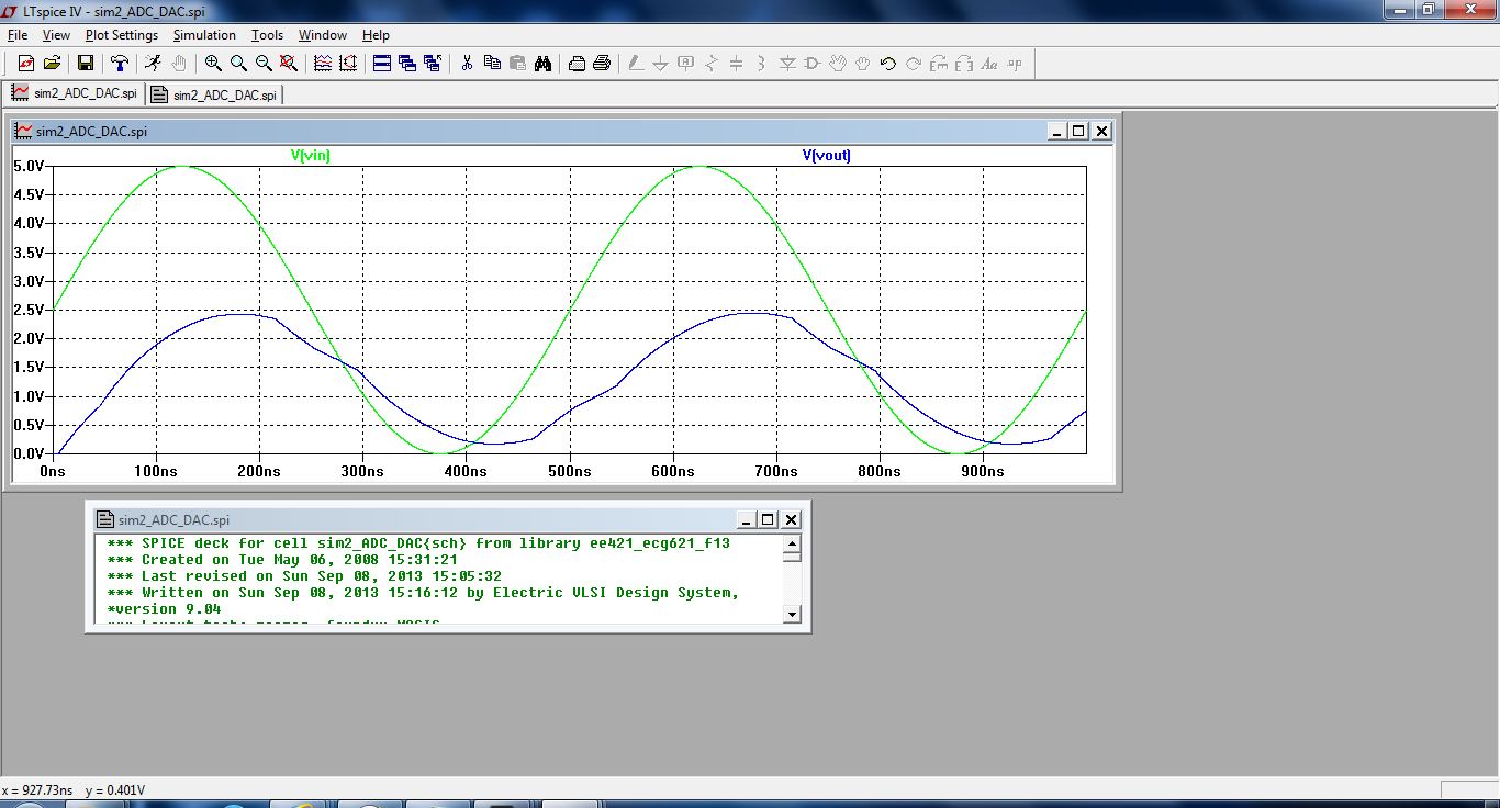
In my own simulation that I performed, I demonstrated how an ADC works, it quantizes the values of the analog signal and
assigns a value to them, so that at its highest point the signal will read all 1 logics, and at its lowest point it will read all 0 logics.
This is illustrated in the picture below showing this exact result.
In order to find the LSB we must divide the Vdd by the number of possible binary numbers.
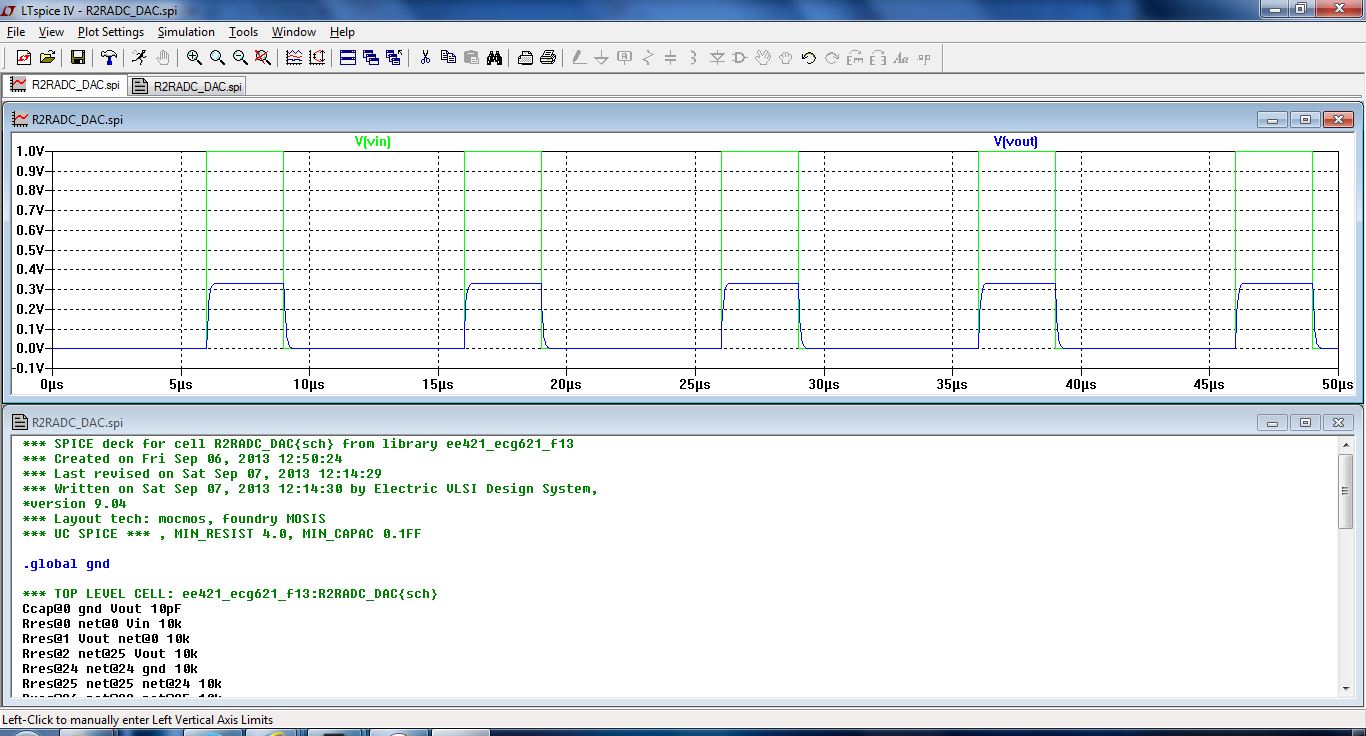
We can now use LTspice's simulation to determine the delay of the output of this DAC using a pulse on the 9th bit.
The delay using a load resistor of 10K results in an expected delay to a half value of 0.7RC or roughly 35 nanoseconds.
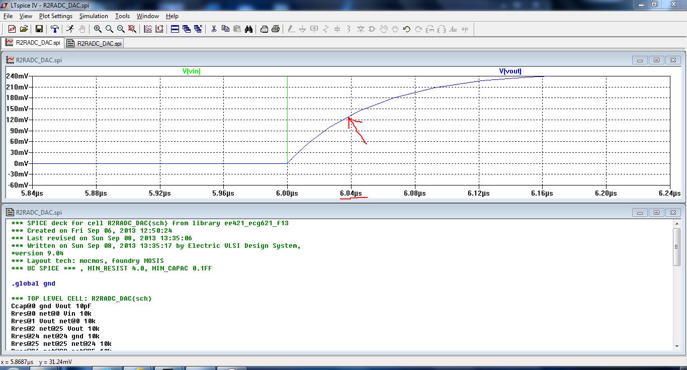
Simulating gives us the results below.
When we zoom in it is easily seen that the approximate time to reach the half value of the final output is 0.7RC, which in this circuit
is about 35 nanoseconds.
Now, instead of just a resistor, only a capactior will be placed at the output.
The result is a smoother signal, but there is a noticeable delay, this delay is caused from the buildup of charge required by
a capacitor, and the slow dissipation of that charge.
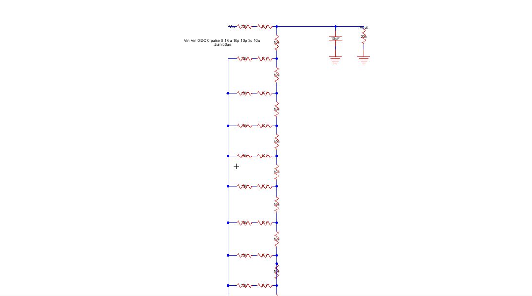
Finally we will show the output when both a 10K resisitor and 10pF capacitor are placed at the output.

discharge very quickly.
Lastly, it is important to realized that our DAC functions with the idea that the switches that provide the logic values from the ADC
has a resistance that is small compared to 10K, if this is proven to be untrue then our values of output resistance will beome unbalanced
and the output values will no longer be as reliable, resulting in some error in our output.