Lab 1 - ECE 421L
Authored
by: Aran Johnson,
Date: 8/30/2013
Email: john1701@unlv.nevada.edu
Lab
description:The program defaults to a grey background color.
Changing
it to a white background will make the printer use less ink. This
can be achieved by going to menu item Window -> Color Schemes ->
White Background Colors
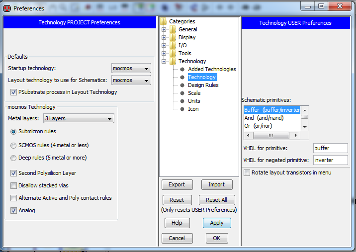
We
will now set Electric up for use in ON Semiconductor's C5 process and
fabrication through MOSIS. This will be done by navigating to
File -> Preferences -> Technology -> Technology to get to the
window below.
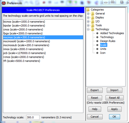
The
scale (lambda) for the C5 process is 300 nm using the MOSIS Scalable
CMOS submicron design rules.
We can set the scale by navigating
to File -> Preferences -> Technology -> Scale and set mocmos
scale to 300 nm.
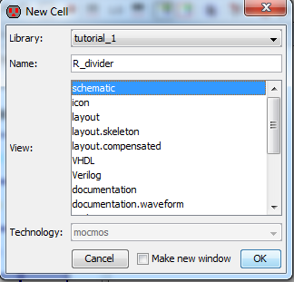
Now
we can draw the schematic of a resistive divider.
Go to Cell
-> New Cell, enter the cell name R_divider and select schematic
as
the view.
You will now see the Components tab on the left side with all of the components.
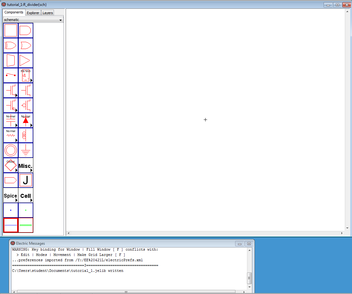
In
the Component menu there is a box with a box containing a resistor and
the word "Normal."
Click on the arrow in this box to place it in
the design area. Fit it into the window using the
zoom buttons.

Edit the properties of the node by selecting Edit -> Properties -> Object Properties to edit
the properties of the node.
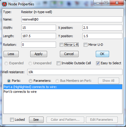
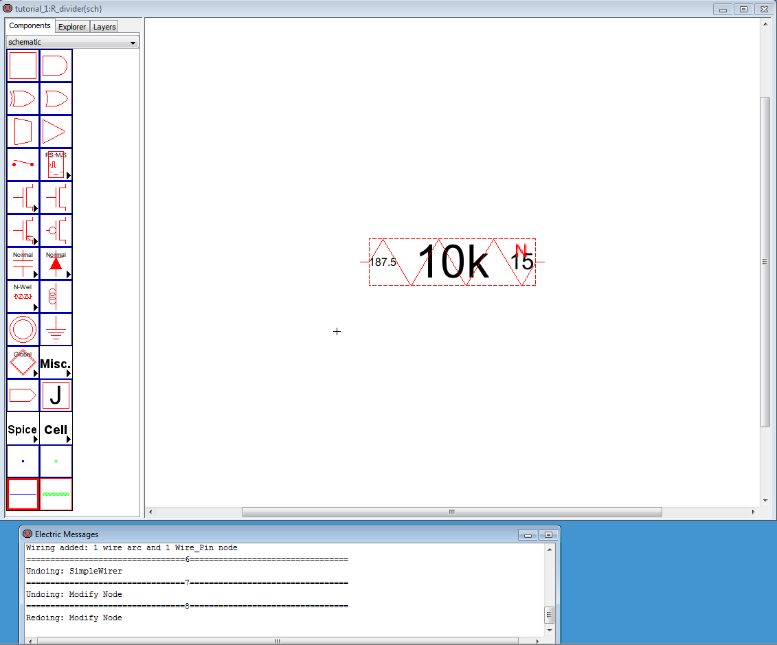
We now see the image below after selecting "OK."
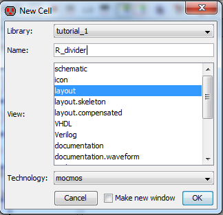
We
can now make a layout that corresponds to this schematic-view cell.
Go to Cell -> New Cell
and enter the Name and View seen below.
Below are the methods I will be using for backing up my files.

return