Lab Project - ECE 421L 

Authored by Fred Hathaway,

hathawa6@unlv.nevada.edu

7 Nov 2013 


Lab Project: Design, layout and simulate an 8-bit ALU that can perform: A AND B, A OR B, A + B (addition) and A - B (subtraction).

In this lab, I used the ALU design from lab 7.  The ALU will have the following inputs (all bus connections): A (8-bits), B (8-bits), F (2-bits) and an output Z (8-bits).

I designed the DEMUX, AND and OR gates in lab 7.  So I used the icons for the ALU design.


AND gate array:

AND_array_icon.JPG 


OR gate array:

OR_gate_array_icon.JPG


DEMUX:

DEMUX_array_icon.JPG


I also utilized the ALU I created in lab 7.

ALU_schem1.JPG


The next step was to put the ALU together in a schematic:  


I needed control inputs to select the different functions of the ALU.  Below is a table woth the control bits:


OPERATIONF1F0
ADD00
SUBTRACT01
OR10
AND11


The ALU schematic with icon view:  The 8-bit inputs for A and B.  The 2-bit control F.  The 8-bit output Z.  

ALU_schem.JPG


I needed to create a new icon.  The clip below shows the correct inputs and outputs.  A (8-bits), B (8-bits), F (2 bits) and the output Z (8-bits).


ALU_icon.JPG


Now for the simulations:

To test the add function, I used binary A=11111110 (0xFE in hex) added to B=00011111  (0x1F in hex). 

The result shows the correct answer:  A+B=00011101 (0x1D in hex).  The control F=0x00.

../proj/ALU_add_wave1.JPG


Now lets simulate the subtraction function of the ALU:

Here I will use A=01011110 (5E hex), B=00110101 (35 hex), F=0x01.  The result shows 00101001 (29 hex)

../proj/ALU_sub_wave1.JPG


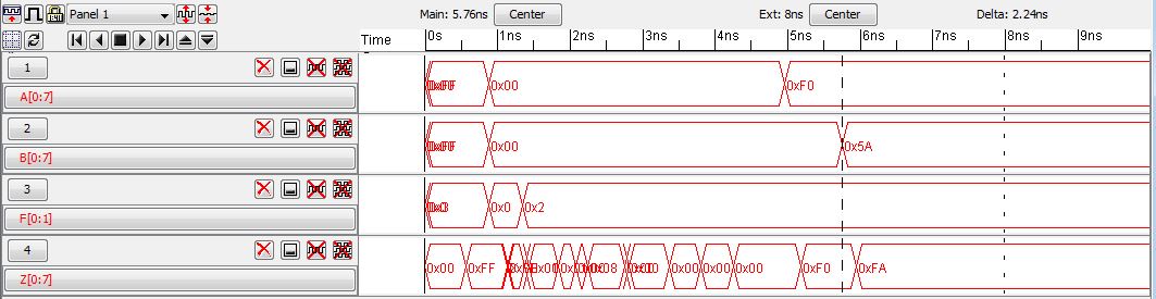
Now for the OR function:

A=11110000 (F0 hex), B=01011010 (5A hex).  The control iput for OR is 0x10. The result of A OR B=11111010 (0xFA hex)

../proj/ALU_or_wave1.JPG


The AND function:

A=11110101 (hex F5), B=01010110 (56 hex).  The control for AND is 11.  The result: A AND B= 01010100 (54 hex)

../proj/ALU_add_wave1.JPG


Layout design:
 
The final layout:
 
AND gate:
AND_array_layout.JPG
 
OR gate:
OR_gate_array_layout.JPG
 
MUX:
DEMUX_array_layout.JPG
 
Inverter:
inverter_array_layout.JPG

Full Adder:
Full_adder_array_layout.JPG
 
ALU Layout:  The measurement is approximately 1500 x 3700 drawn.  
ALU_layout2.JPG
 Closeup of top section:
ALU_%20closeup1.JPG
 
Closeup of bottom section:
ALU_%20closeup2.JPG
 
Simulations:
 
To test the add function.  I used hex values, A=0xFE, B=0x1F and F=0x00.  The result Z=0x1D as expected.
ALU_add_wave2.JPG
 
To test the subtract function.  I used A=0x5E, B=0x35 and F=0x01.  The result Z=0x29.
ALU_sub_wave2.JPG
 
To test the OR function.  I used A=0xF0, B=0x5A and F=0x02.  The result Z=0xFA.
ALU_or_wave2.JPG
 
To test the AND function.  I used A=0xFE, B=0x1F and F=0x11.  The result Z=0x1E.
ALU_and_A_wave2.JPG
 

I backed up my lab work by archiving directory, emailing and posting on the cmosedu website.

Copy of Lab_Project_fh_13.jelib file
 
Return to EE 421L Labs