Lab 8 - ECE 421L Digital Design Lab
Medhanie Petros, Petrosm@unlv.nevada.edu
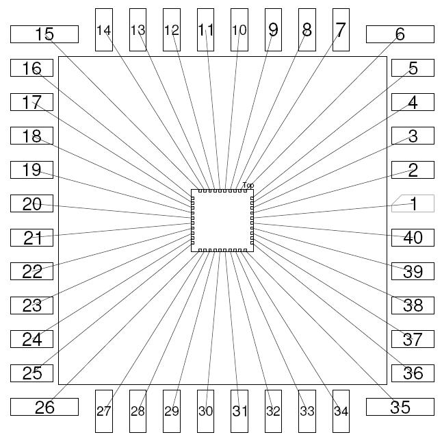
We will be using a 1.5mm x 1.5mm chip with 40 bond pads.
GROUND WILL ALWAYS BE Pin20
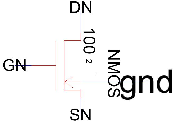
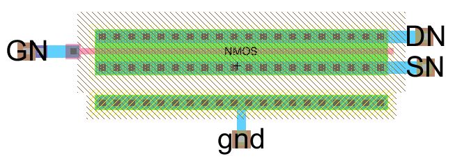
Test Structure
-Connect ground and Sn to pin 20
-Apply small gate voltage to pin23
-Measure Drain current on pin22
DN-Pin22
SN-Pin21
GN-Pin23
Body-Pin20
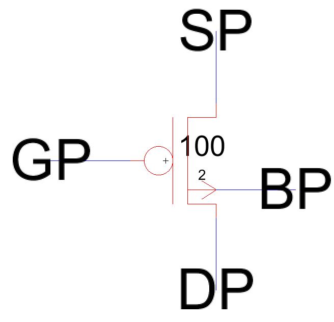
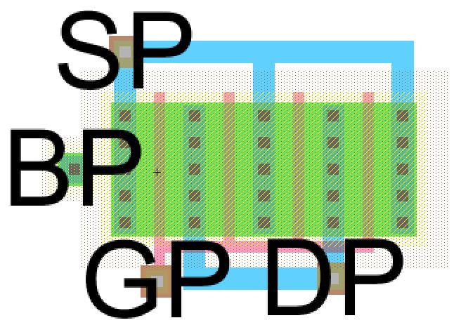
PMOS 100/2
Test Structure
-Connect vdd of 5v to Sp and to pin 25
-Apply small gate voltage to pin26
-Measure Drain current on pin27
SP-Pin24
DP-Pin27
GP-Pin26
BP-Pin25
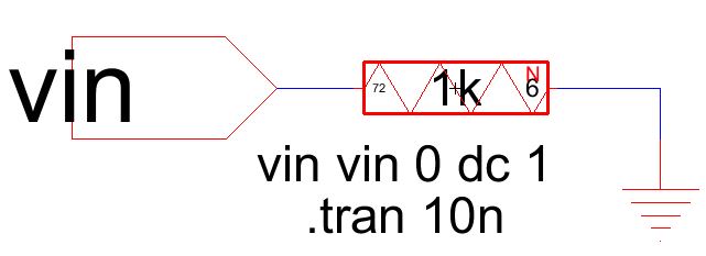
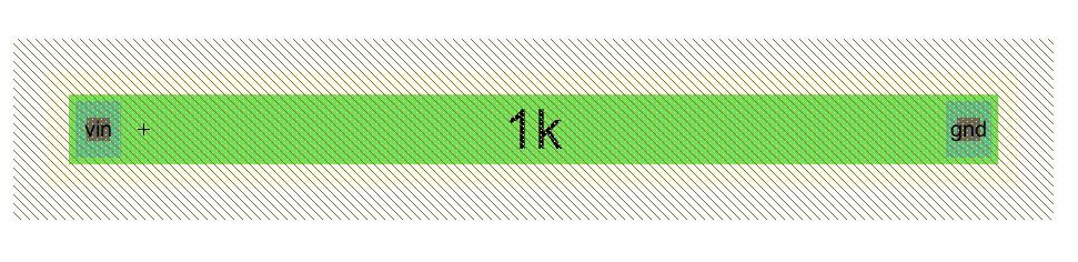
1k n+ resistor
Test Structure
-Ohm meter from pin 2 to pin 20 = 1k
Vin-Pin2
Ground-Pin20
1k p+ resistor
To test structure
-connect vdd of 5v to pin40
-connect any voltage < 4v to pin 1
-Rout is internally connected to Pin 20
Pin-Pin1
Nwell-Pin40
Ground-Pin20


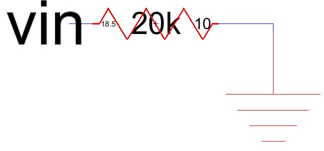
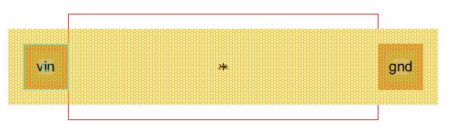
20k n-well resistor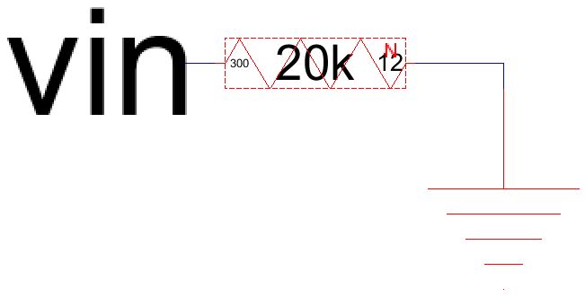

20k hi-res poly2 resistor
Test Structure
-Ohm meter from pin 32 to pin 20 should= 20k
Vin-Pin32
Bandgap reference
To test structure
-connect vdd of 5v to pin33
-connect ground to pin20

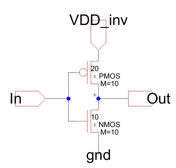
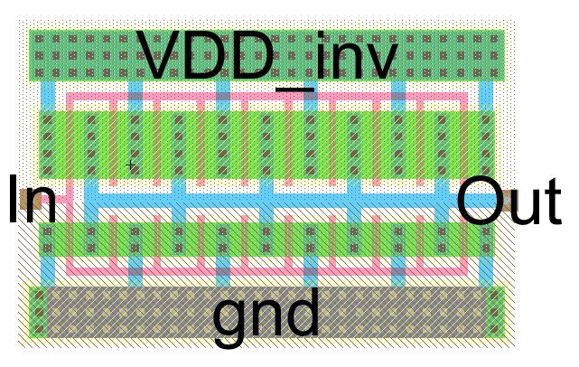
Inverter
Test Structure
-Connect gnd to pin20
-Pulse low frequency to pin 30
-Measure pin 28
Power-Pin 29
In-Pin30
Out-Pin28
61 stage ring oscillator
To test structure
-connect vdd of 5v to pin39
-connect ground to pin20OSC_out-Pin38
OSC VDD-Pin39


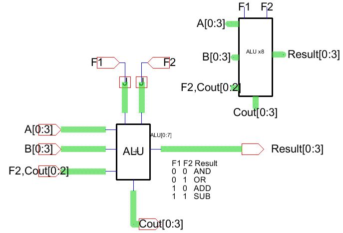
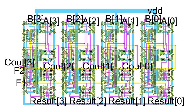
ALU_4Bit
Test Structure
-Connect gnd to pin20
| F1 | F2 | Result |
| 0 | 0 | AND |
| 0 | 1 | OR |
| 1 | 0 | ADD |
| 1 | 1 | SUB |
A[7:0]=1100 (12)
B[7:0]=1010 (10)
Bi[7:0]=0110 (+246,-10)
| A and B | A or B | A + B | A - B |
| 1000 | 1110 | 0110 (22) | 0010 (2) |
Vdd-Pin10
F1-Pin19
F2-Pin18
A0-Pin8
B0-Pin9
A1-Pin11
B1-Pin12
A2-Pin13
B2-Pin14
A3-Pin15
B3-Pin16
Result0-Pin7
Result1-Pin6
Result2-Pin5
Result3-Pin4
Cout3-Pin17
To test structure
-connect vdd of 5v to pin35
-connect ground to pin20

AND Gate


Final Product 40 pin Chip

