Lab 4 - ECE 421L
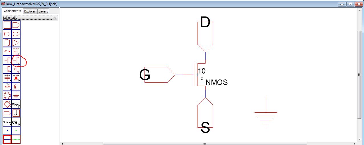
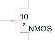
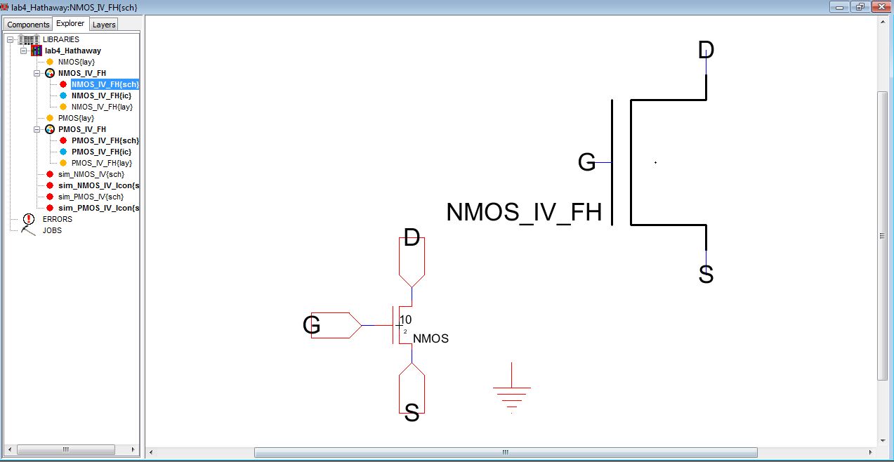
I changed the width to 10 and the length is set to 2.
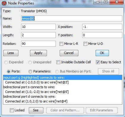
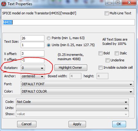
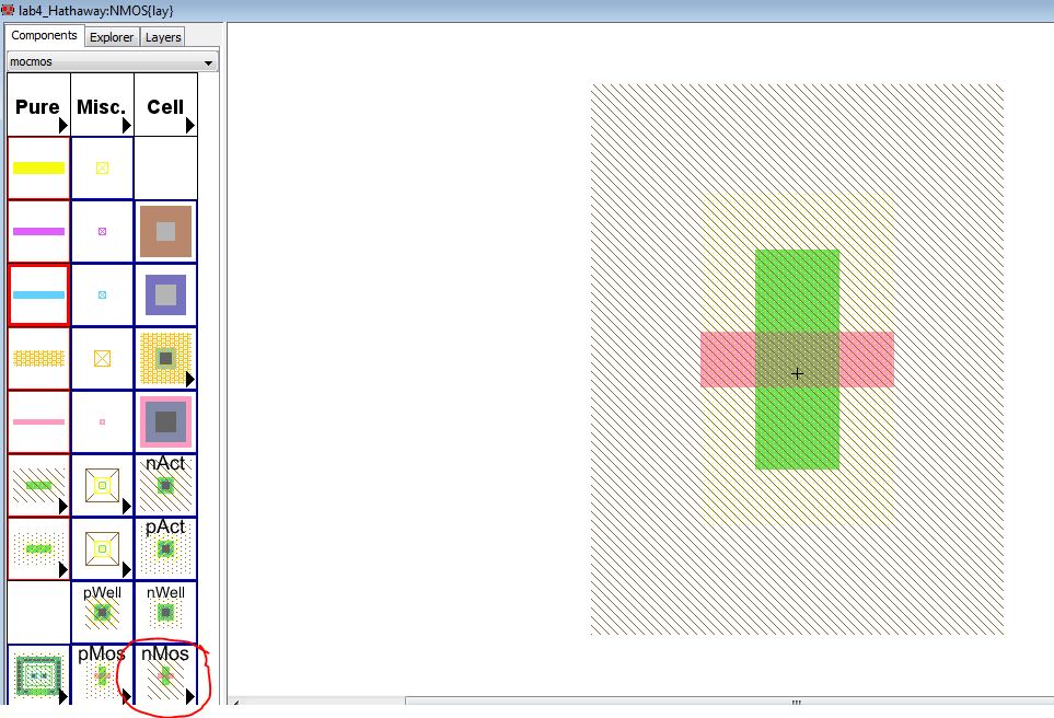
Next I selcted the NMOS node and went to Tools -> Siulation (Spice) -> Set Spice Model. We can rotate the text as desired through the device properties. I chose to leave a 0 degrees orientation. I used the device prperty menu and changed the "Spice Model" to the one for our design which in this case is "NMOS".
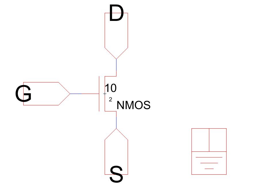
Once the device properties are set I cleaned up the schematice by placing the text next to the device. At this time I created three nodes (from component menu) and labeled the D,G and S as shown below. Additionally, the ground is placed as seen below.
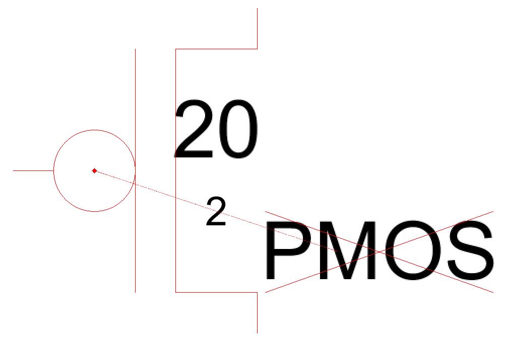
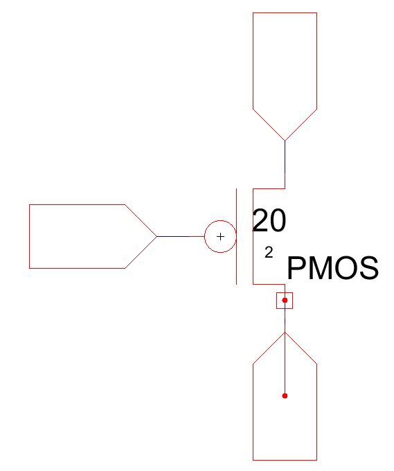
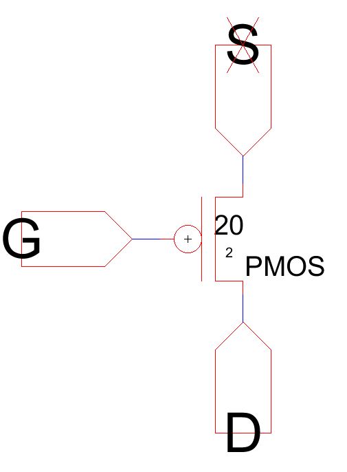
Added the wire and exports. Added the "Spice Model" and changed it to "PMOS" in the device properties menu.
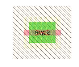
Next add metal1 contact to poly1 as seen below. This will connect the metal1 to the MOSFETs gate terminal. Additionally, select the pWell Node for the body connection. Your layout should look like this now:
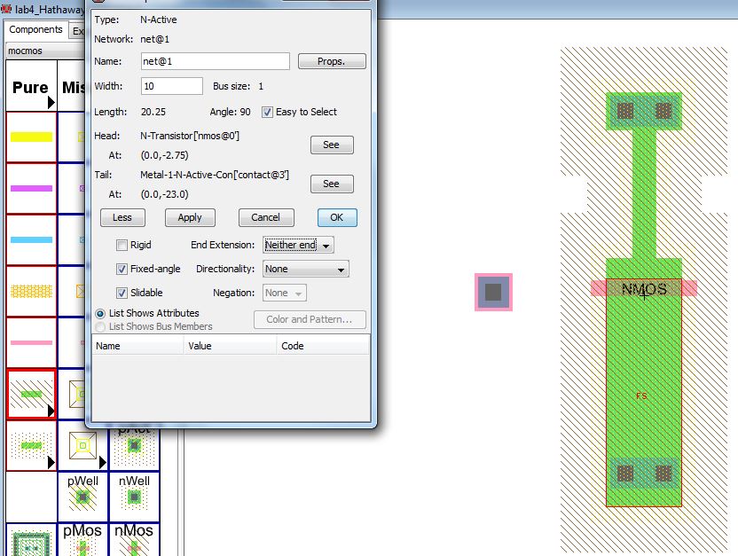
Select the nMOS node and click Edit -> Properties -> Object Properties (or CTRL_I). Set the width to 10 like we did in the schematics. Next with the nMOS node still selected go to Tool -> Simulation (Spice) -> Set Spice Model. Set the Spice model and change it to NMOS to match the schematic that we created earlier. Also, make sure you change the text size to a readable size like 2.
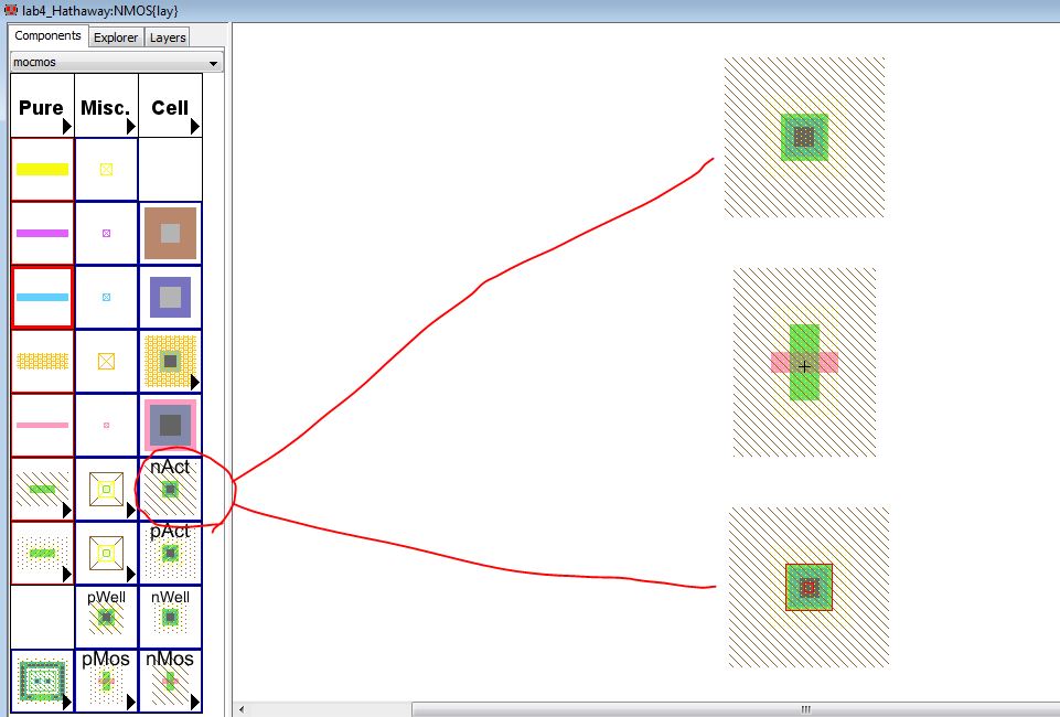
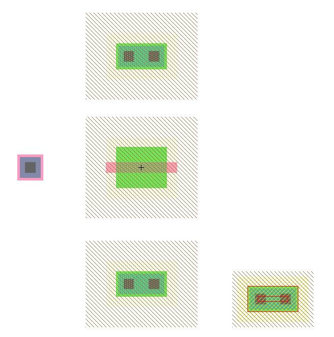
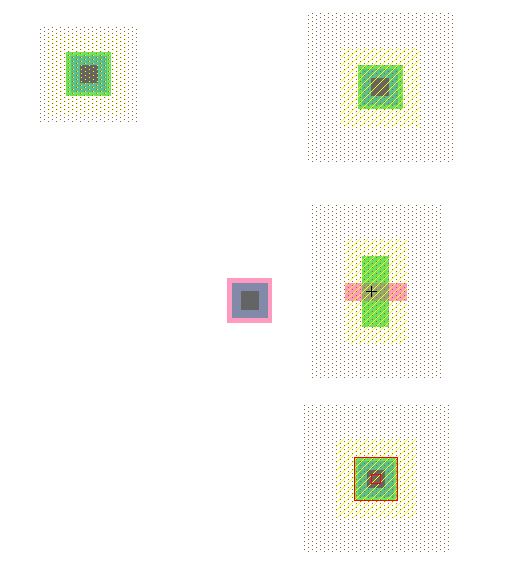
We also need to change the size of the nAct Nodes. You can select both by first selecting one and the hold shift while selected the second node. Edit properties with CTRL-I. Change the X size to 10. We also need to change the size of the pWell node.
Next, we need to connect the nMOS node to the nAct node. Do this by left clicking on the nMOS node and righ clicking on the nAct node. Do the same for the other nAct node. Change the width of the arc to 10 and select Neither End for the End Extension.. Results are seen below:
Now move the top and bottom nAct node into place:
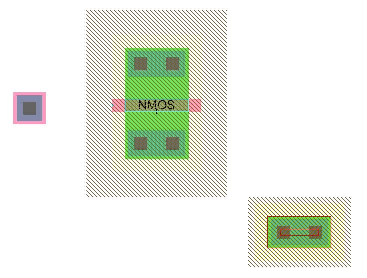
Make sure you check for DRC errrors (F5). If you have any errors, make sure you correct them.
Next we will connect the gate of the MOSFET to the poly1 to metal1 node. Once connected I had to change the width to 2 in order for the arc to match the width of the nMOS node.
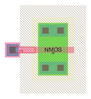
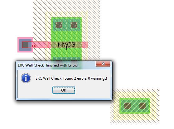
At this time when we do a ERC Well Check (Tools -> ERC -> Well Check) we will get two errors. This is because there is no well contact to the p-well surround the NMOS device and the pWell node is not connected to ground.
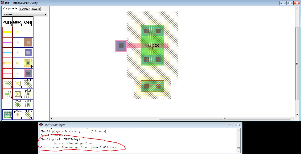
Move the pWell node over so that it overlaps the nMOS pWell layer. Now do another Well Check and ensure there are no errors.
Next lets connect the substrate to ground. Left click on the pWell node and right click below to create an arc. Create an export (CTRL_E) and label it gnd.
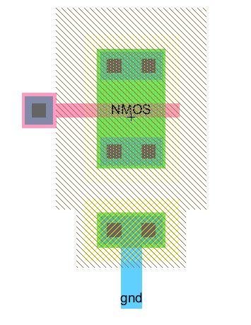
Next add metal1 arcs to the other 3 terminals and create exports as well. Check for DRC and well errors.
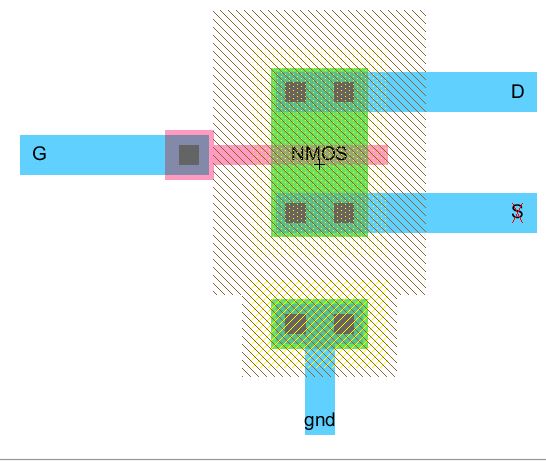
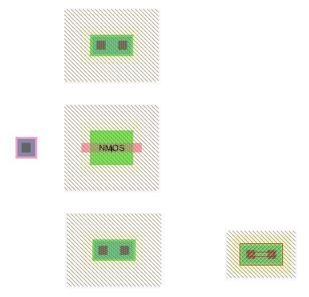
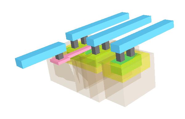
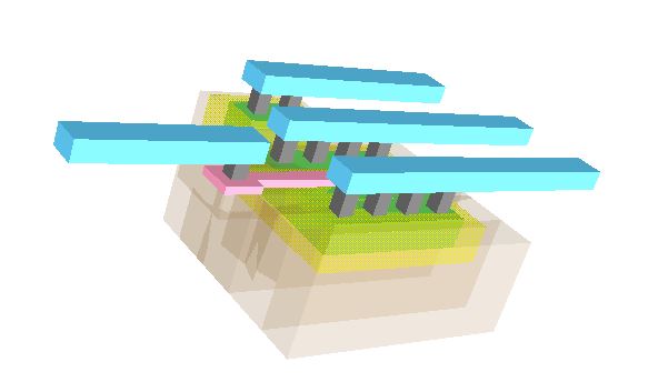
3-D view of the NMOS device:
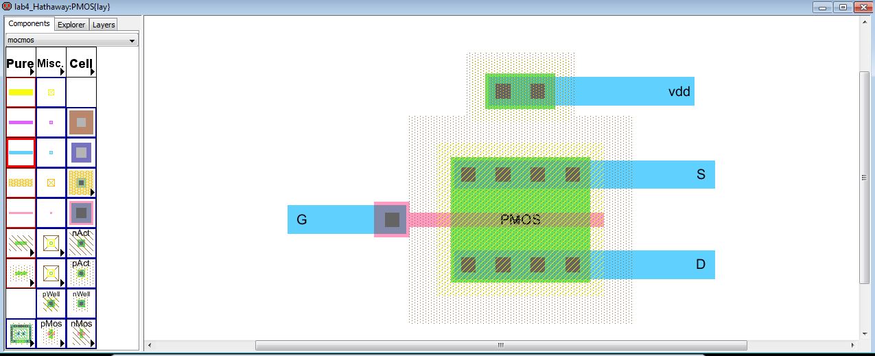
Save the library. Next create the PMOS_IV layout in a similar fashion. Select pMOS node, 2 pAct nodes, nWell node and metal1 to poly1 contact.
Below is the PMOS layout with the exports ( D, G, S and vdd).
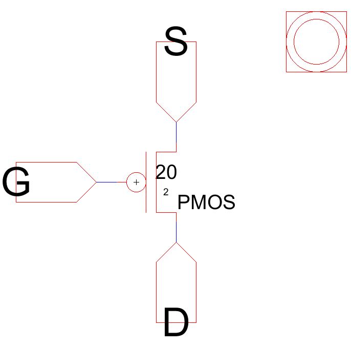
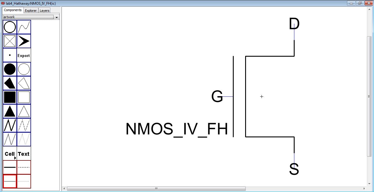
Next, I created icons for my design to simplify the look of the schematic. To create an icon select your schematic that you created for the NMOS device, go to View -> Make Icon View.
A generic box appears in the corner of the schematic. You enter the icon view my selecting the icon and press CTRL-D. This will enter the icon editor. Here I selected created the icon using the various shapes from the component list. Once I drafted the icon the way that I wanted, I moved the exported over and placed them in the correct orientation. Below is my NMOS icon design:
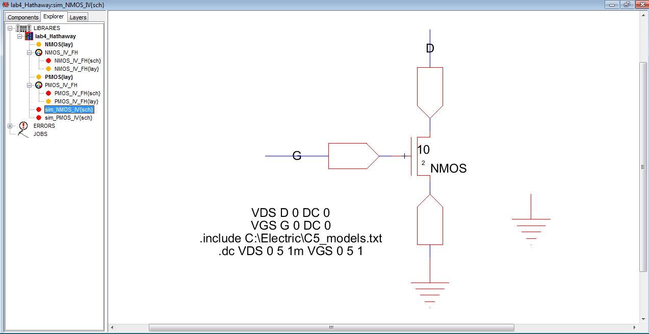
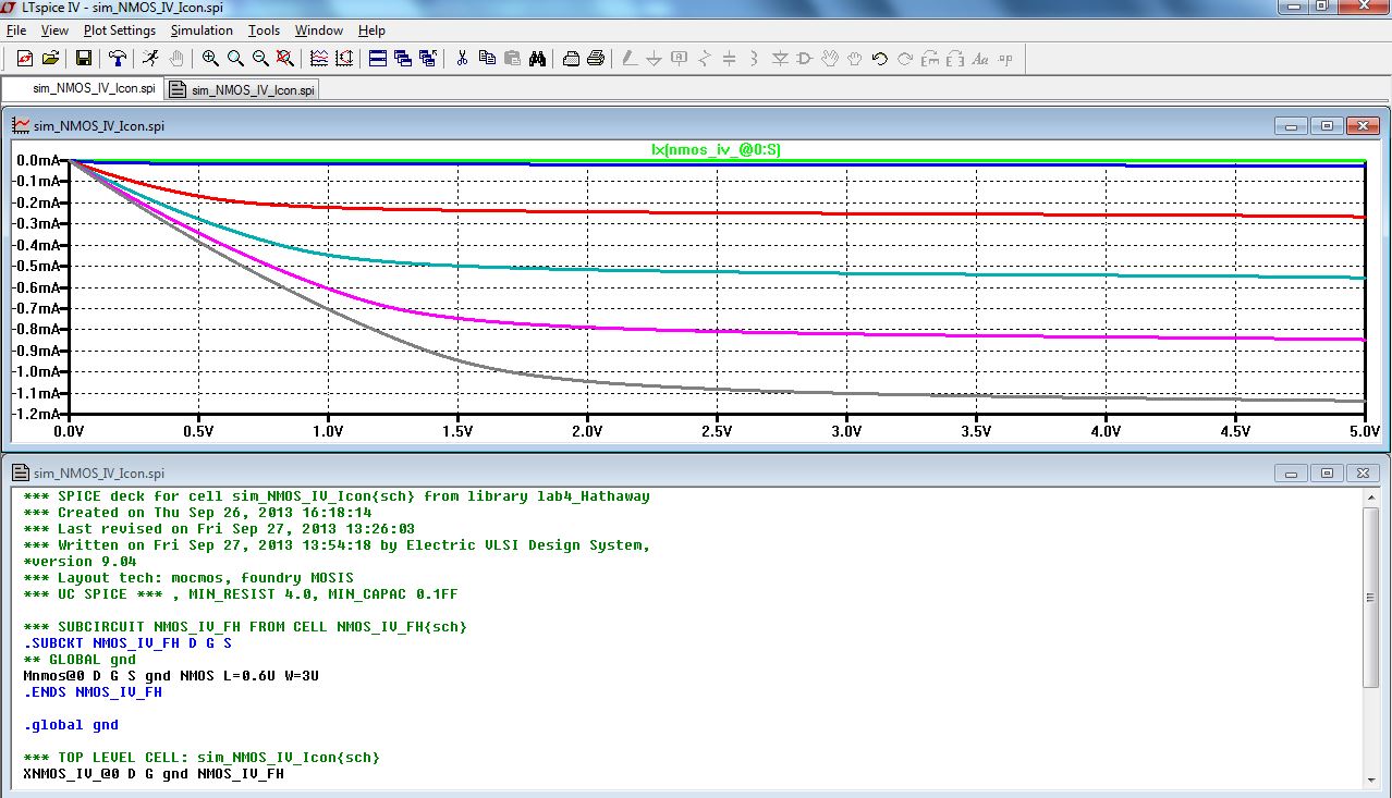
Now that the icon for the NMOS device is completed. I can use the icon in my simulation schematic seen below:
![]()
The simulation results for the NMOS device:
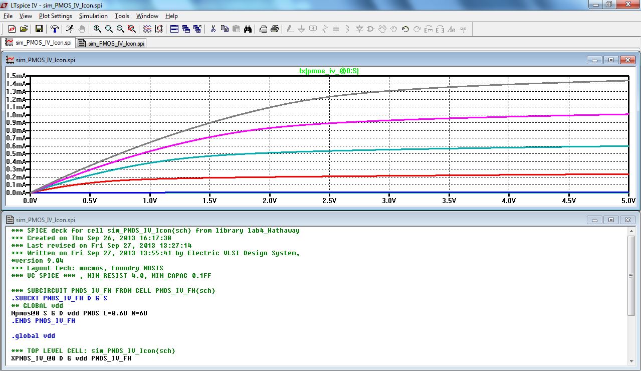
PMOS icon: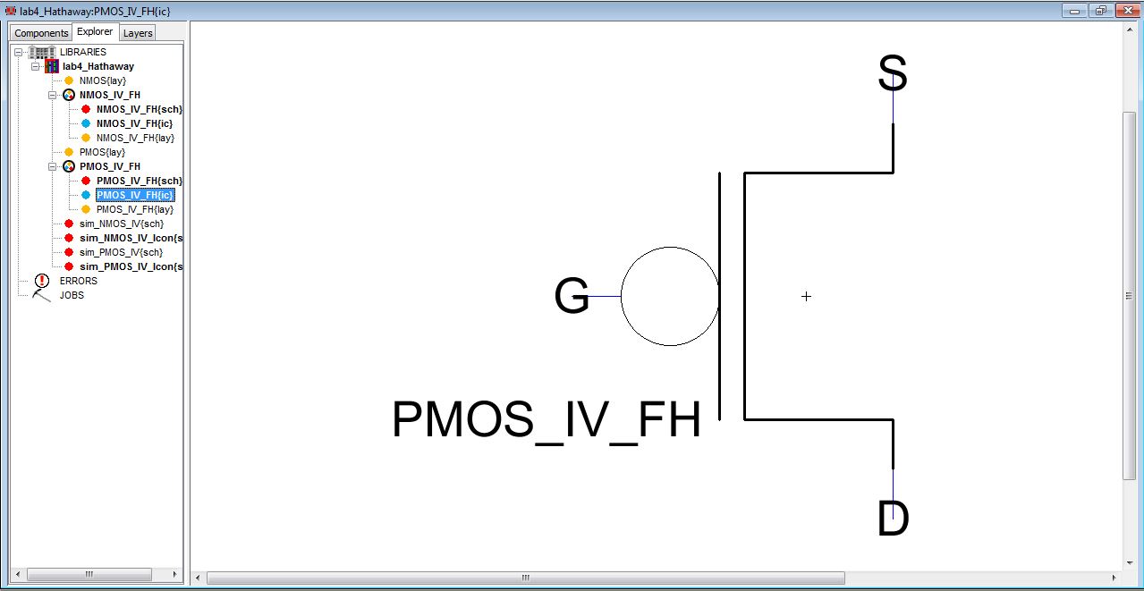
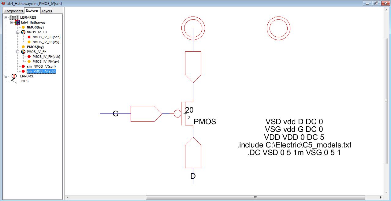
I also used my PMOS icon in my simulation schematic. The look is much better now:
![]()
PMOS simulation results: