Lab 3 - ECE 421L
I completed the tutorial 1 for Electric as seen below.
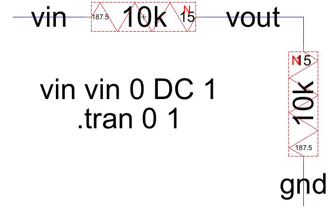
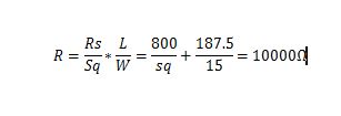
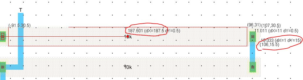
This clip shows the schematic of the resistor divider from tutorial 1. Note that the length of 187.5 and the width of 15 is shown on the resistor. These are annotated by clicking on the resistor and pressing ctrl-I to edit the parameters. Additionally the resistor value is allow annotated the same manner. The wires are drawn by right click, left click of the mouse.
Once the schematic is complete check for errors by pressing F5. A common error is unnecessary pins. This can be cleared by going to Edit->Cleanup cells-> Cleanup pins everywhere..
To label the arcs highlight arc and press cntl-I to edit the properties. Or simply double click on the arc.
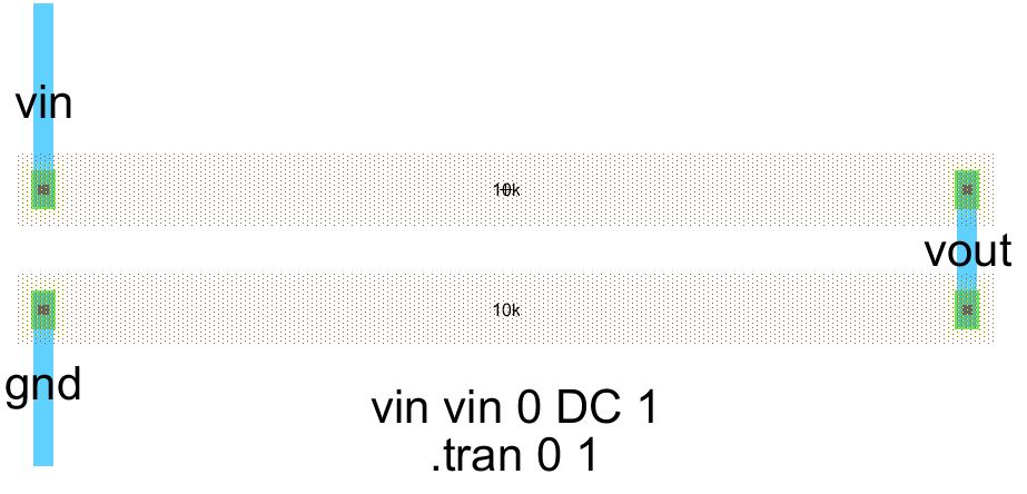
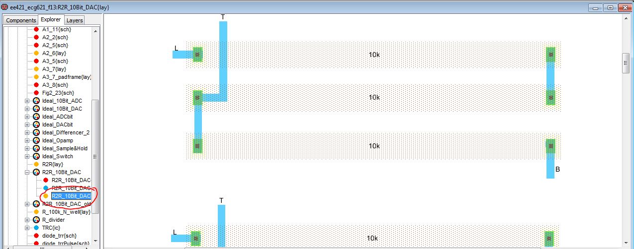
A layout design was created by cell-> new cell and selecting layout. The scale of 0.5 was selected for grid alignment. Note that the exports are on metal 1.
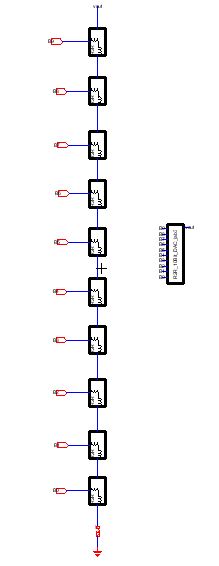
Lab 3: layout of 10-bit DAC.
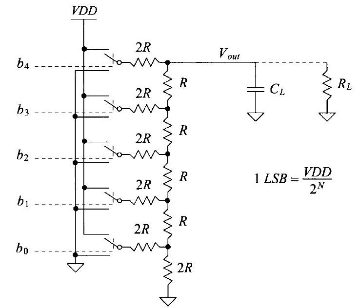
I will be designing a layout of a 10 bit DAC similar to the following picture:
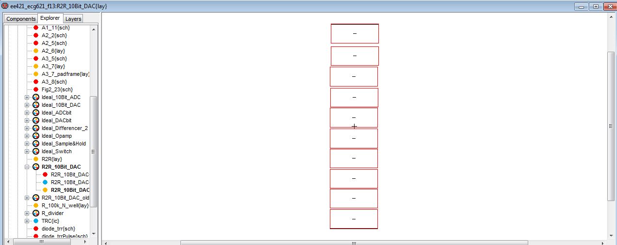
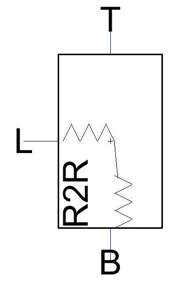
I created a cell consisting of three resistors in series. This is one cell of the resistors. Note that the exports are on the metal 1 layer.
The next step was make 10 copies of the cell as seen below:
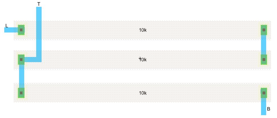
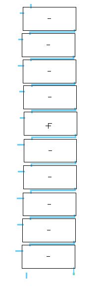
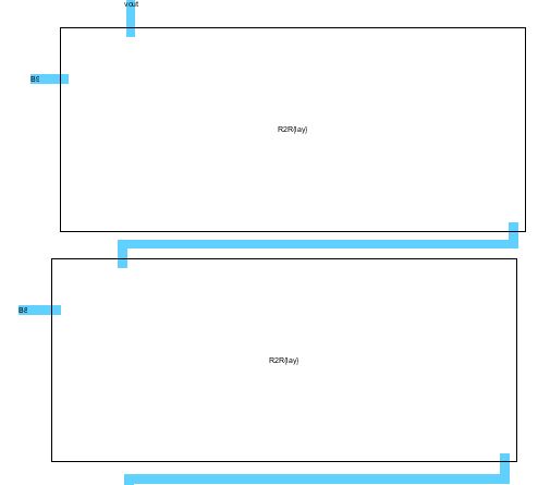
Final layout of the 10 cells connected.
Closeup of top cells:
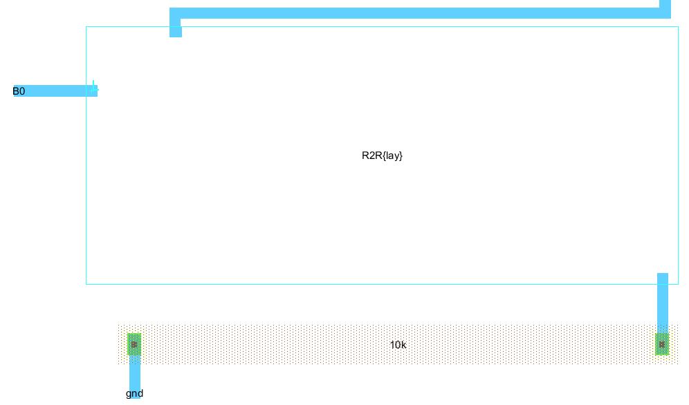
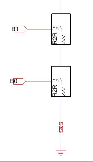
Last cell with a 10k resistor:
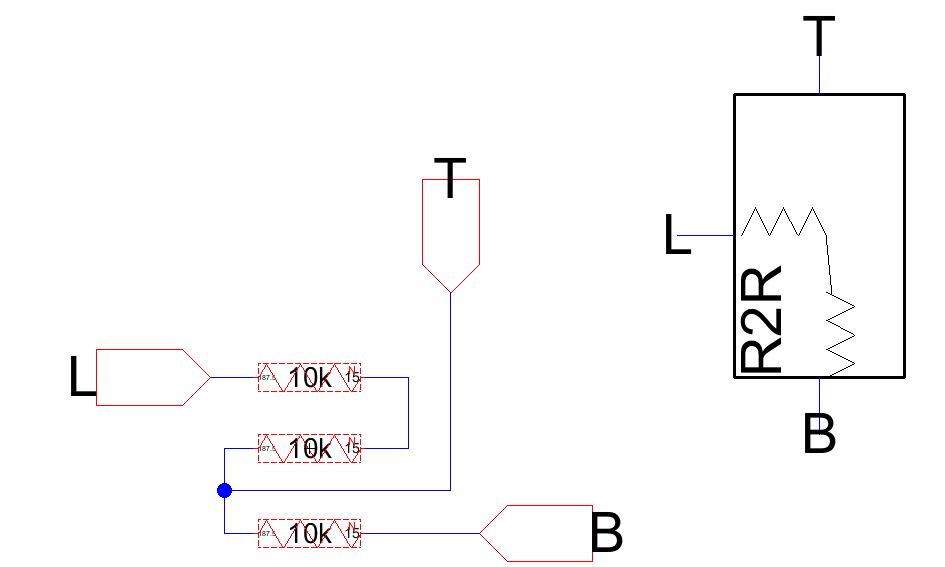
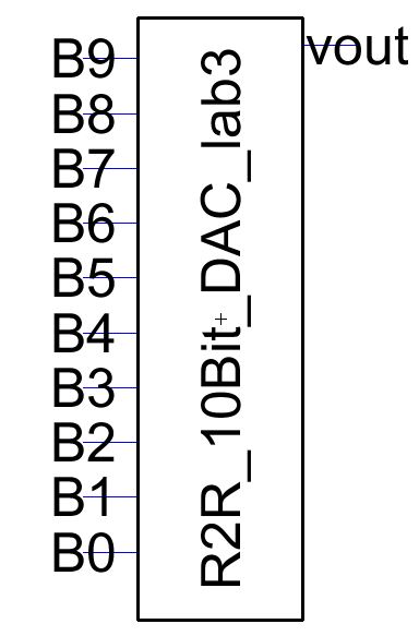
I created an icon of for the schematic. Click ->View ->Make Icon View.
Schematic view of cell with icon:
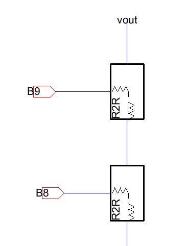
Last two with 10k resistor:
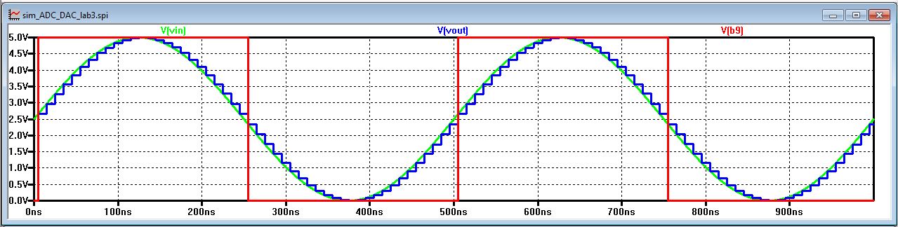
I created a schematic to view the simulation results and verify the operation of the DAC:
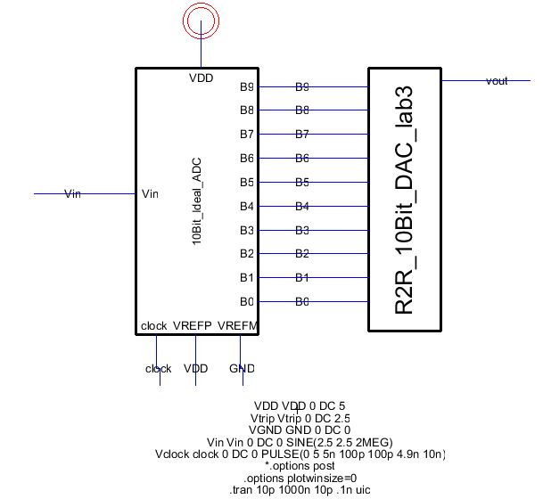
The simulation results are shown below (VIN,VOUT, and VB9. The results are comparable to the results from lab 2. The input is a sinusoid and the output is not as smooth as the input and is stepped due to the Digital to Analog conversion.