Lab 2 - ECE 421L
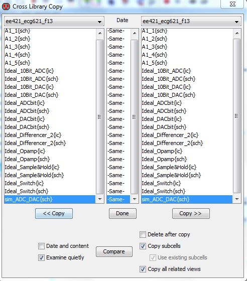
I downloaded lab2.jelib file to my Electric directory. Next I opened Electric with the ee421_ecg621.jelib and lab2.jeli files. I then clicked in Cell -> Cross-Library Copy and followed the prelab directions.
As
seen above, I copied sim_ADC_DAC{sch} and all of the subcells and the
related views into ee421_ecg621.jelib. Once completed, it clicked
done to exit this screen. The jelib was saved by clicking on disk
icon in upper right corner of Electric. I then backed up the
jelib files by zipping and emailing a copy to myself.
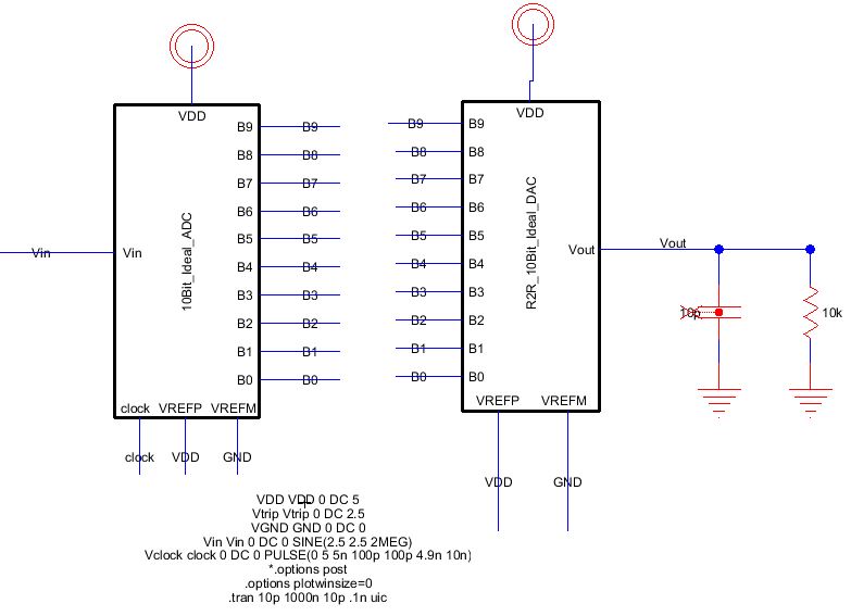
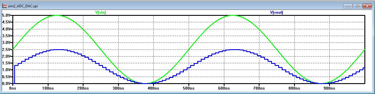
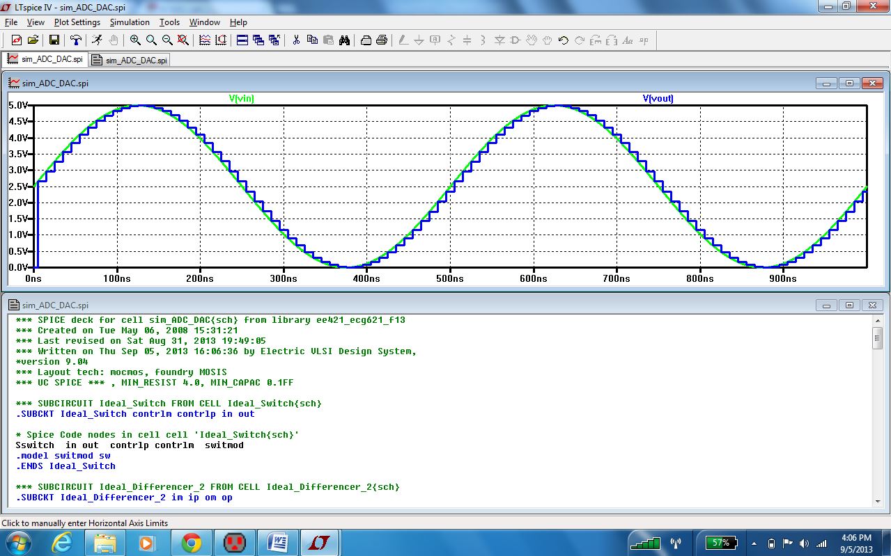
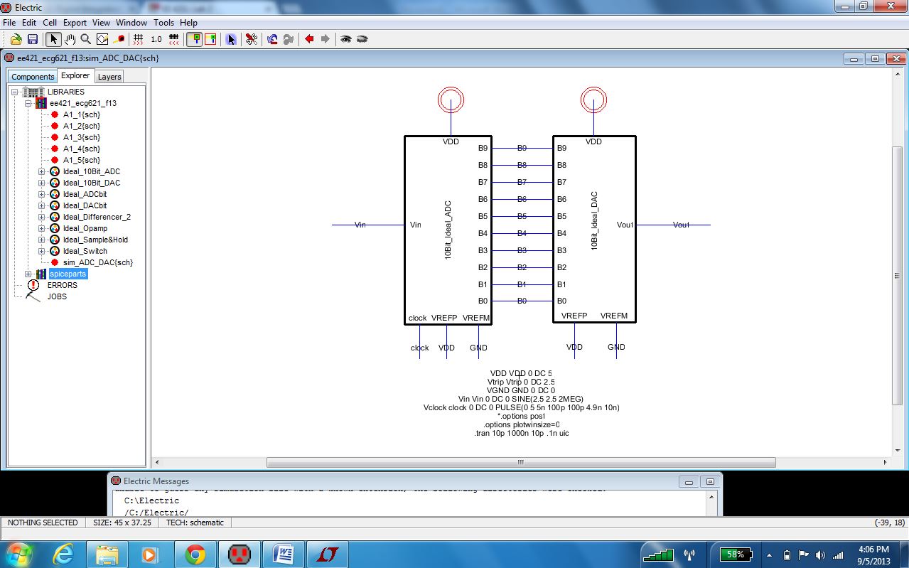
Next, I opened up the sim_ADC_DAC{sch} schematic and ran the simulation.
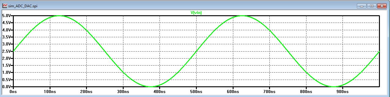
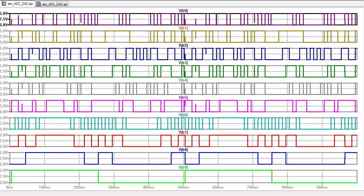
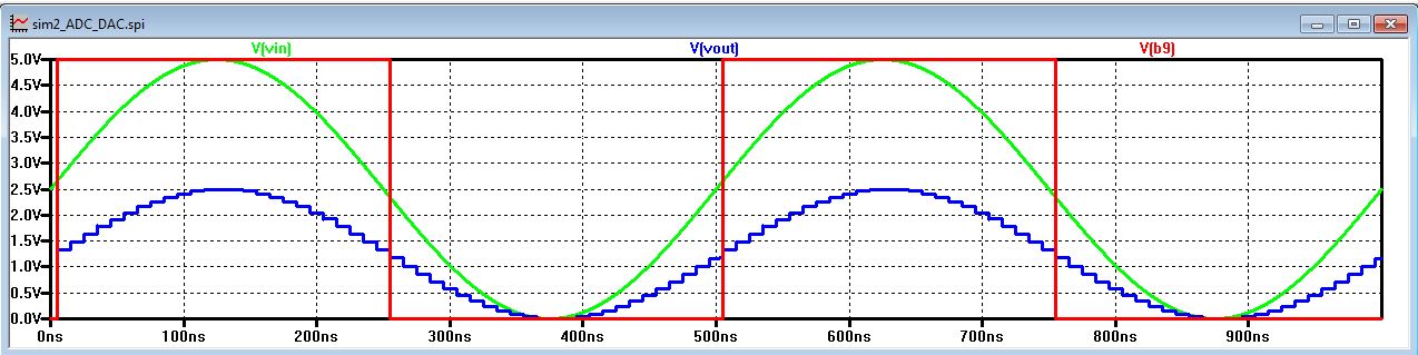
The signal is the n converted into a digital signal. The more bits, the better the resolution.
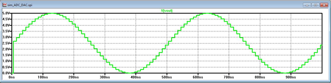
The digital signal is then converted back into an analog signal. The input the the DAC is a binary word of 10 bits and the output is an analog signal. The converted signal is not as smooth as the original analog signal. For each digital input there will be a corresponding output as shown below. This explains the steps in the wave form. The more bits the input has, the smaller the steps of the output signal. This is referred to as resolution.
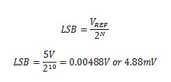
The least significant bit (LSB refers to the right most bit
in the digital word. The LSB defines the
smallest possible change in the analog output voltage. The LSB will be annotated as D0. In this case the LSB is 4.88mV.
PostLab:
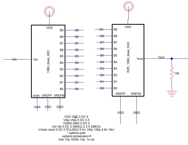
The design of a 10-bit DAC using an n-well R of 10k:
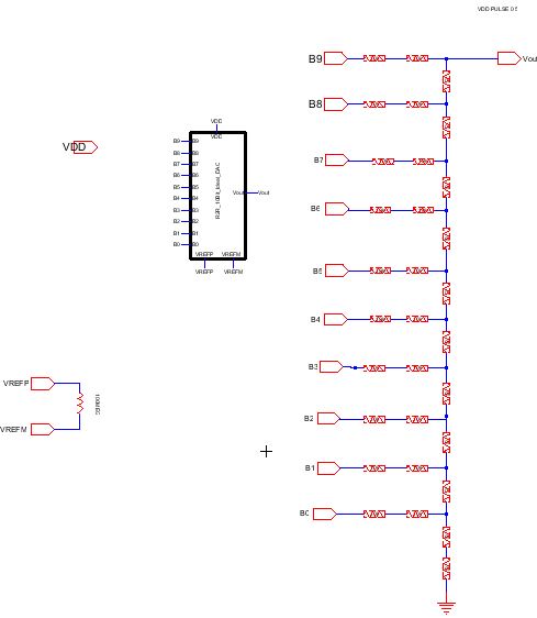
As seen above this design is implemented using 2 separate 10k resistors in series. After checking for design rule errors, I had to clean up the cell in electric by edit->cleanup cell->cleanup pins everwhere. The eliminated some of the errors. The next step was to do an auto stitch by clicking tools->routing->auto stitch.
Driving a 10pF load:
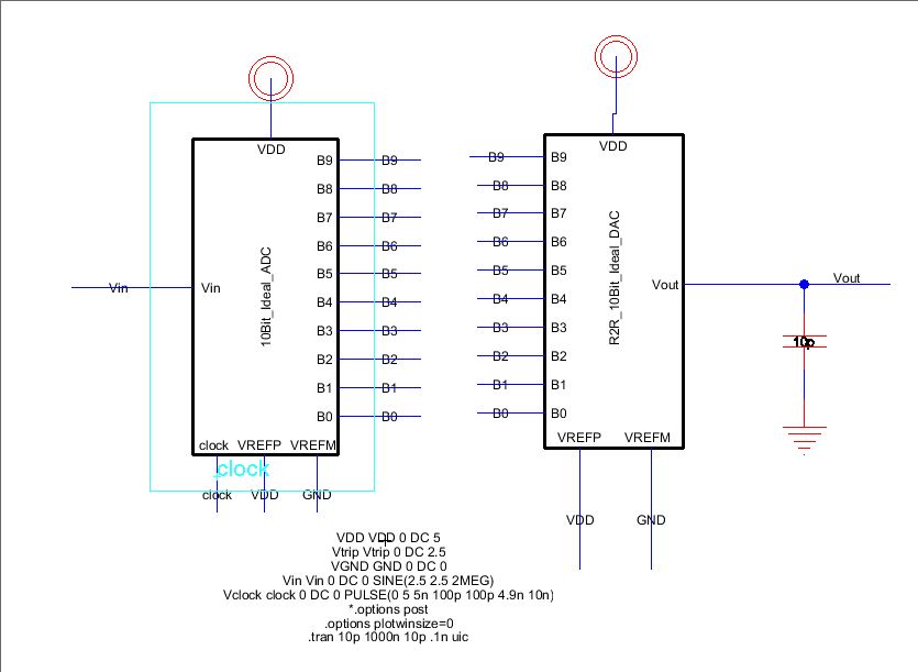
All of the DAC inputs are grounded except for pin B9. We just want to see what happens to one input and verify the time delay is 0.7RC.
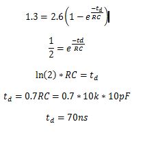
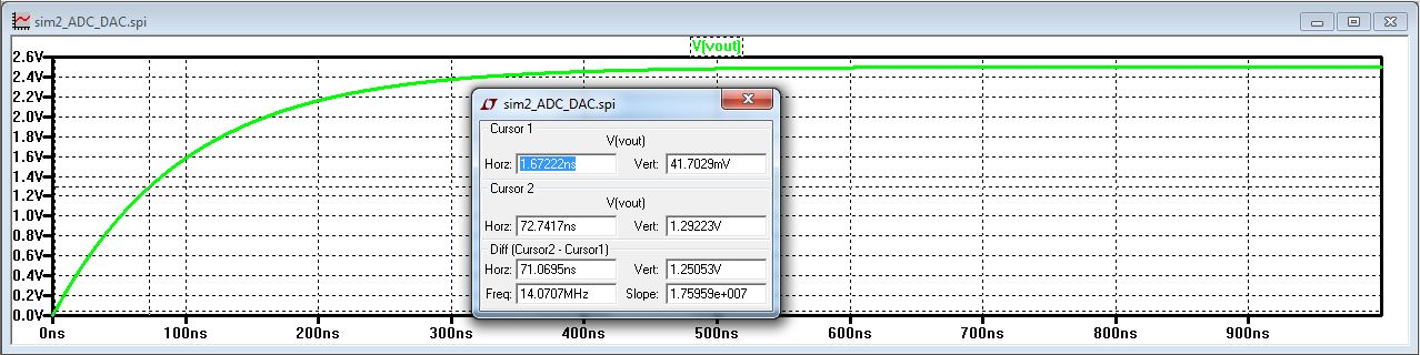
As seen in the figure above the difference between cursor 1 and 2 is 71ns which is a close match to the calculated time of 70ns.
Once the design is completed we can create our own icon in Electric by edited icon view. Highlight the device that you want to create an icon.
![]()
![]()
Simulations of the R2R DAC:
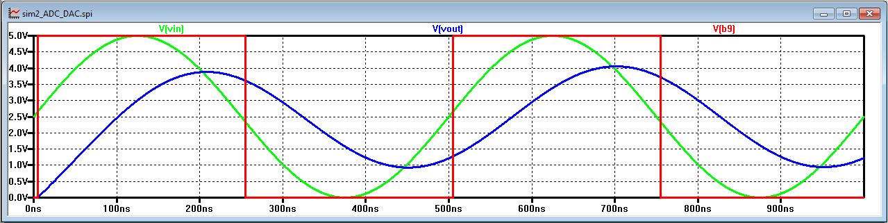
With 10k load:
Wave form with 10k load:
With the 10k load we see that the amplitude drops and we see the steps in the output.