Lab 1 - ECE 421L
Authored
by Fred Hathaway,
29 Aug 2013
Lab
description:
Lab
1 is a tutorial on how to edit webpages following the lab 1 tutorial.
In addition we will be configuring and starting Electric based on tutorial 1.
Figure 1: The following clip shows Electric with default settings.
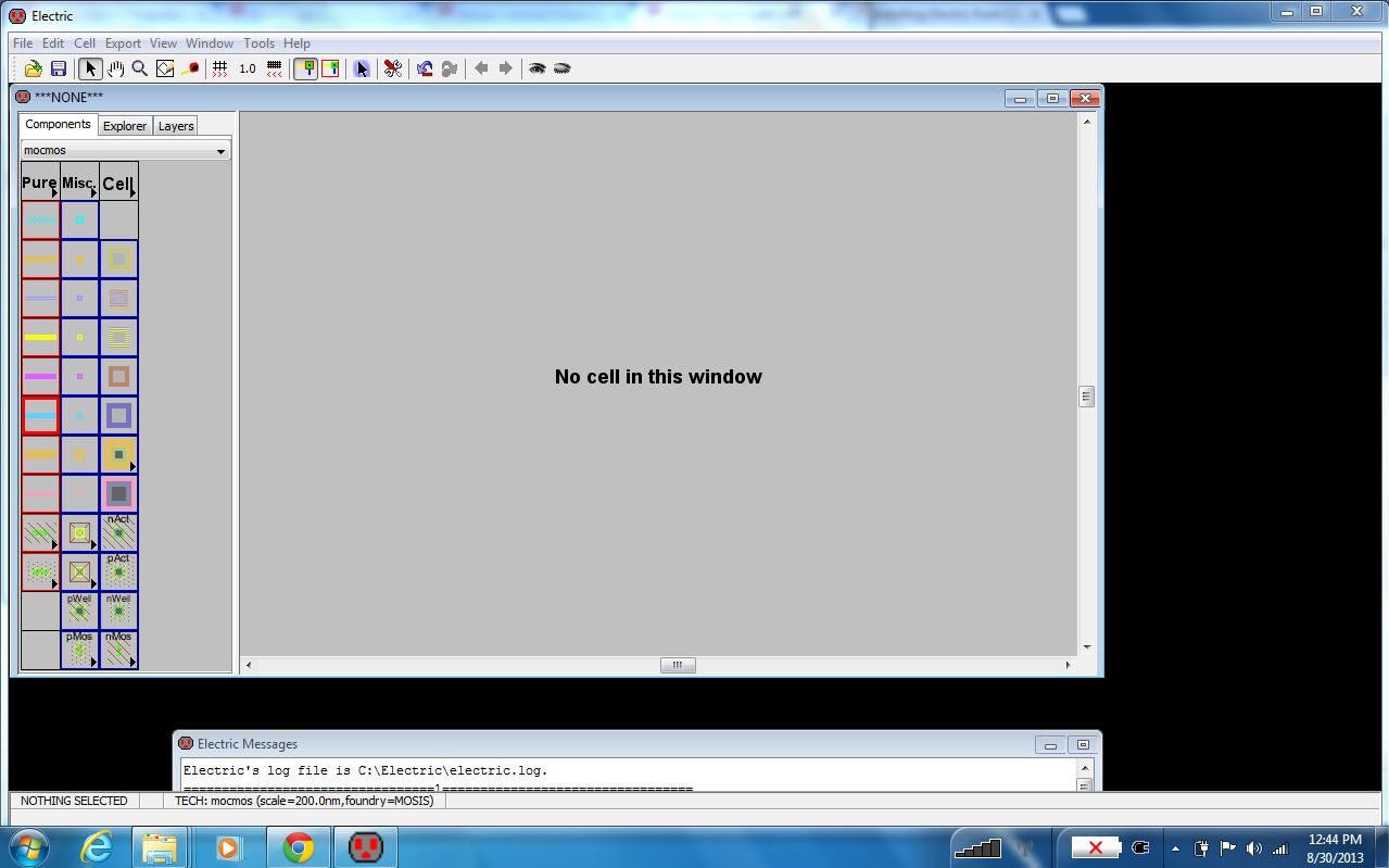
Figure 2: Screen clip of Electric after setting Color schemes to white background.
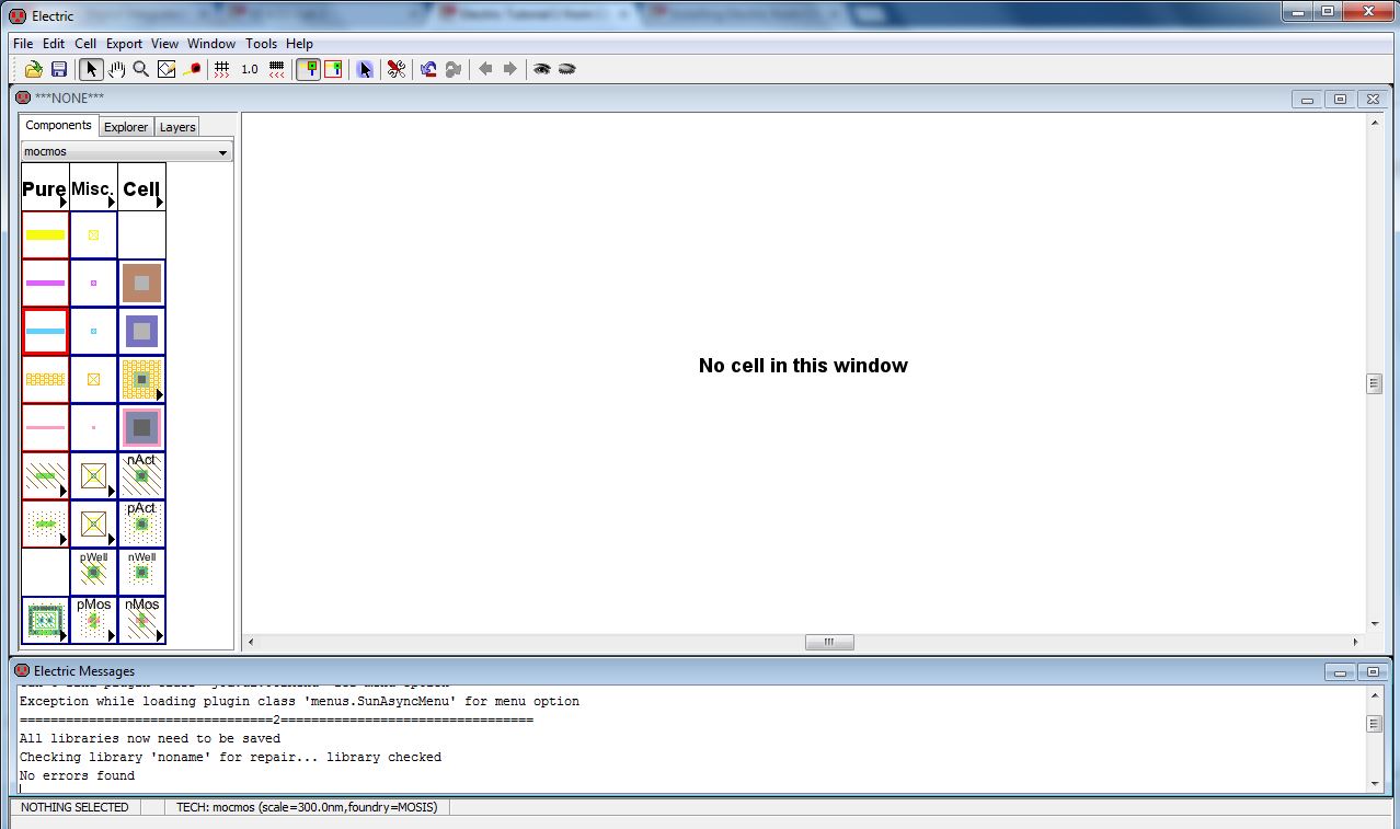
Figure 3: Screen clip after setting technology preferences using ON semiconductor's C5 process and fabrication through MOSIS.
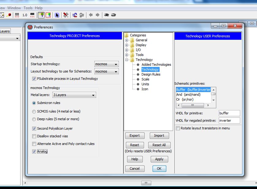
Figure 4: Screen clip after mocmos scale set to 300nm.
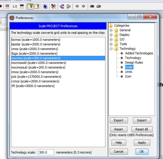
Figure 5: Screen clip showing new cell begin created,
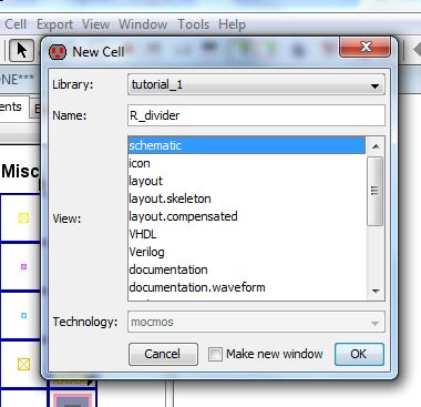
Figure 6: N-well schematic resistor shown in drawing area.
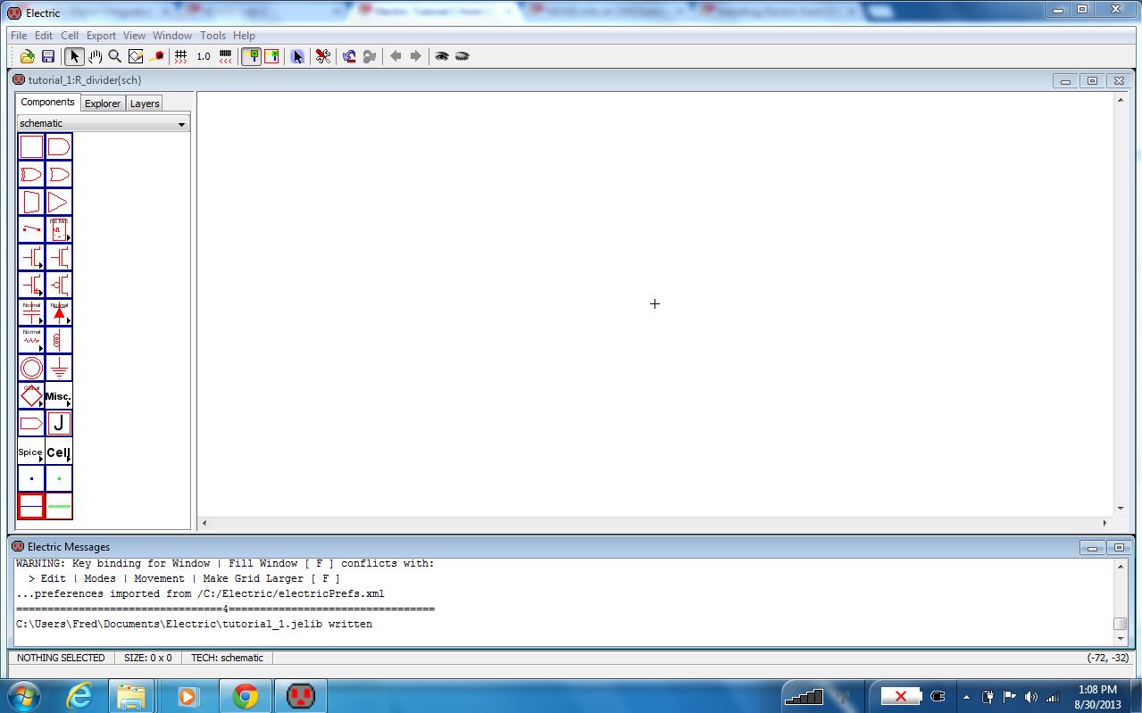
Figure 7: Clip showing Node object properties.
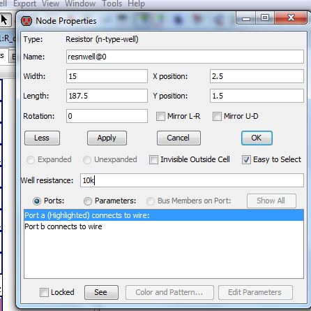
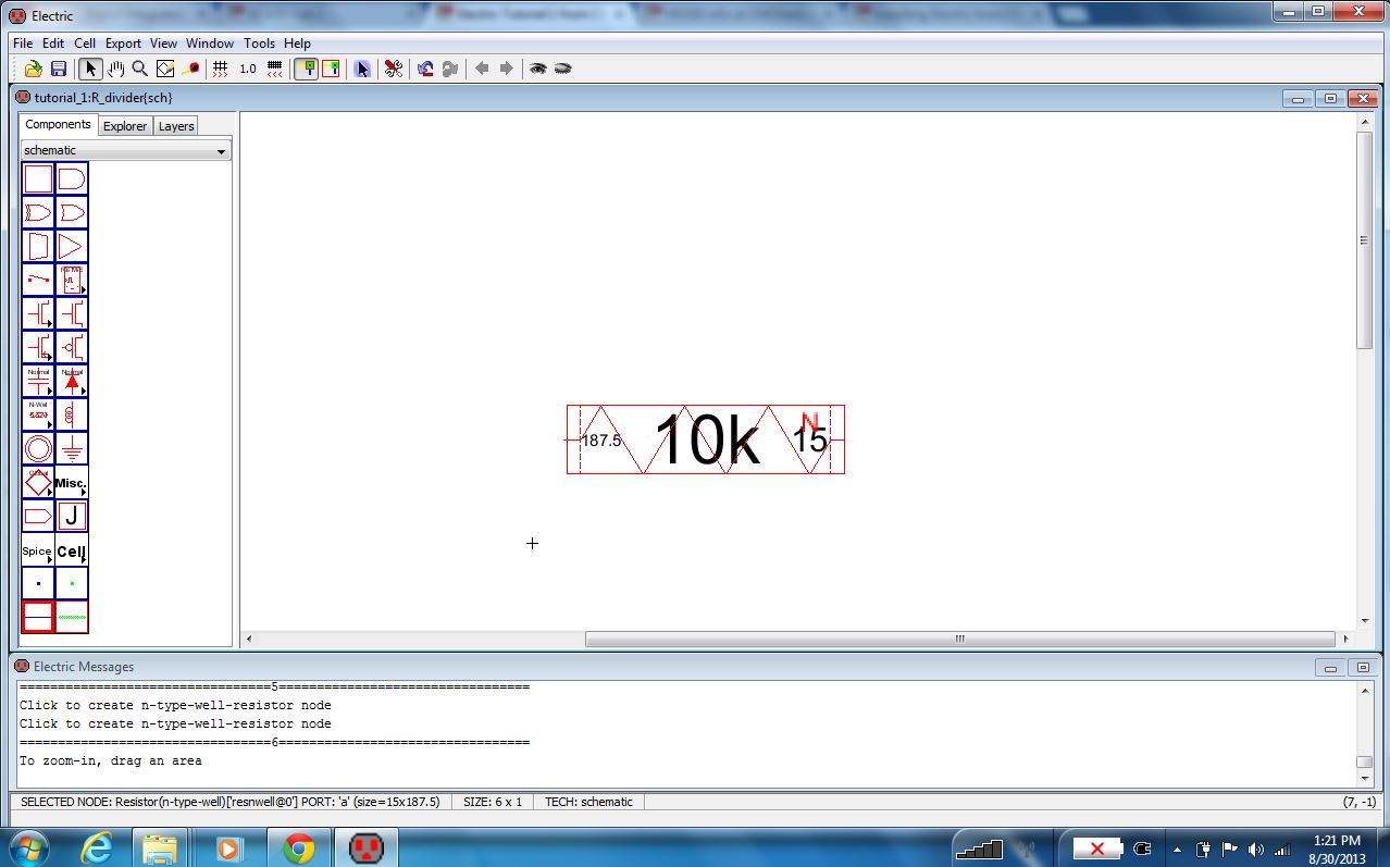
Figure 9: 10k N-well resister after changes.
2.
I performed regular backups by zipping and emailing files.
Additionally, I edited the webpage on my desktop folder and
copied files over to the ftp server.
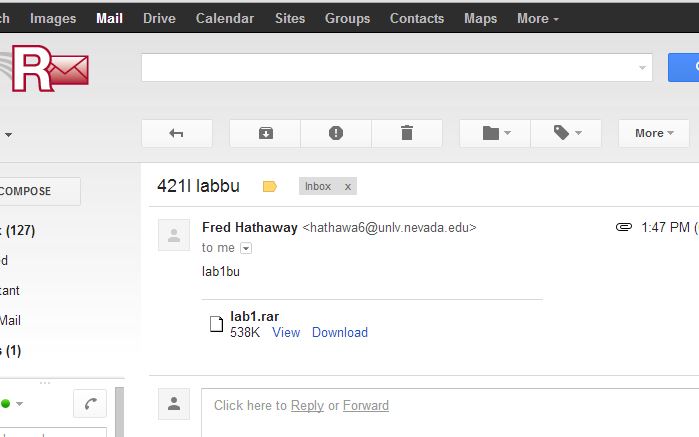
Figure 10: Clip showing zipping files prior to emailing to myself.
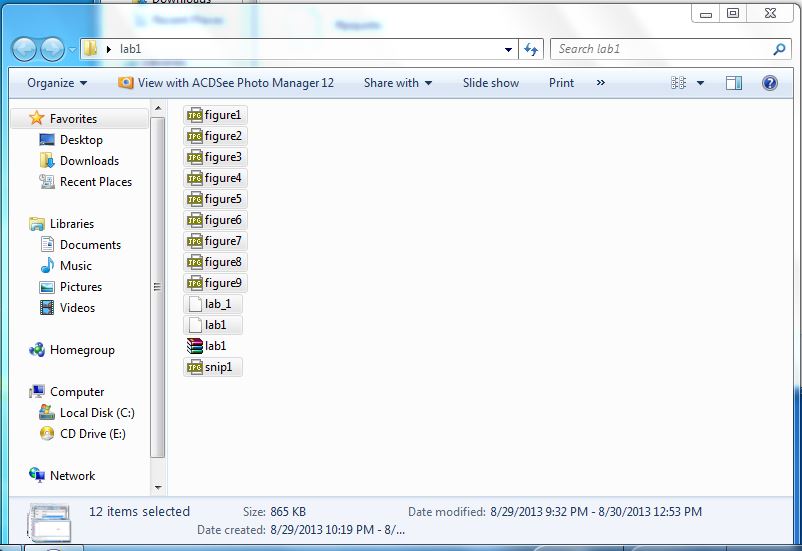
Figure 11: After emailing zipped backup to myself.
ee421_ecg621_f13.jelib
Return to EE 421L Labs