Lab Final - EE 421L
Authored
by: Kendrick De La Pena
Date: November 6, 2013
Email: delape19@unlv.nevada.edu
Lab Description
Lab Final will create a functioning ALU unit using parts created in the previous lab
Lab Work
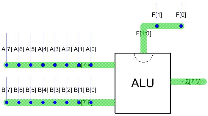
The
ALU has three inputs: A[7:0], B[7:0], and F[1:0]. A and B are used as
the values for input while F is used for selecting the operation.
F = (0,0) = A + B
F = (1,0) = A - B
F = (0,1) = A OR B
F = (1,1) = A AND B
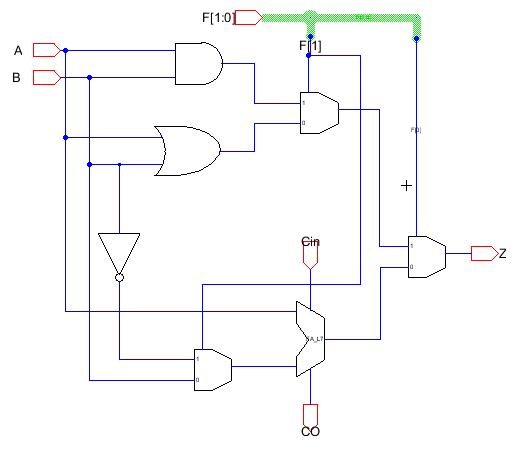
Shown below is the schematic. It uses 3 demuxes, 1 AND gate, 1 OR gate, 1 inverter, and 1 Full Adder.
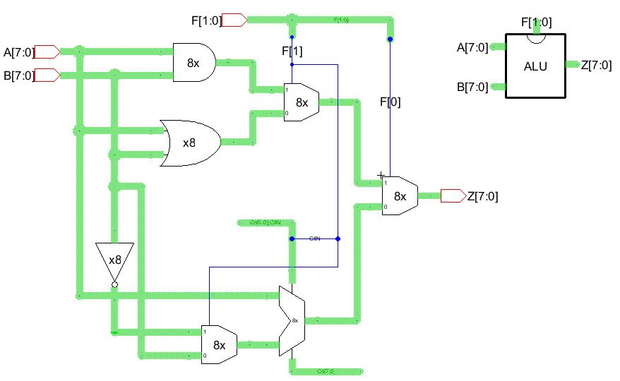
When
F[0] = 0, then the full adder is selected. If F[1] = 0, then B is
selected, added to A, and Cin is 0. If F[1] = 1, then B is inverted,
added to A and Cin is 1.
When F[0] = 1, the Demux is selected, and F[1] = 1 selects AND while F[1] = 0 selects OR.
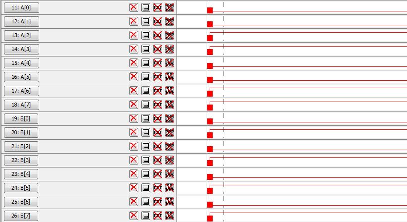
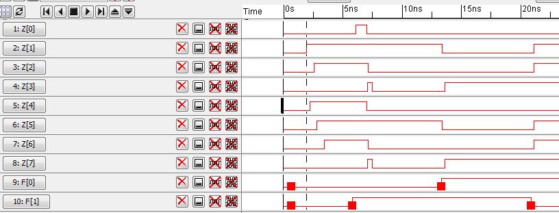
Here is the IRSIM showing the input and output. A = 1100 1100 and B = 1010 1010.
If F = (0,0), then A+B = 0111 0110
If F = (1,0), then A-B = 0010 0010
If F = (1,1), then A AND B = 1000 1000
If F = (0,1), then A OR B = 1110 1110
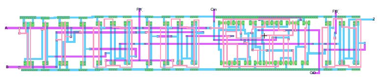
Layout
First
step is to create the ALU for 1 bit. The schematic and layout are below
(NOTE: Layout is hard to see. Open corresponding file)
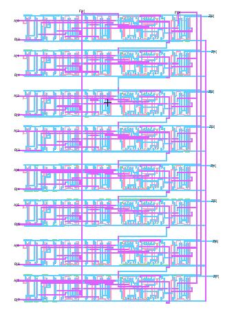
To
create the 8 bit layout, simply copy the 1 bit layout eight times.
After, connect all vdd and gnd to each other. Each A, B, and Z ports
will be number 0 through 7. F[1] and F[0] will all be tied together.
Layout is below
Return to Kendrick's labs