Lab 8 - ECE 421L 

Ian Yanga - yangai@unlv.nevada.edu

Ruben Medina - medina72@unlv.nevada.edu

Kendrick De La Pena - delape19@unlv.nevada.edu

Nolan Moore - mooren14@unlv.nevada.edu


December 6, 2013


Prelab

- Download and cross library copy the bare pads for a tiny-chip (1.5mm x 1.5mm with 40 bond pads) seen 

 
Lab
- Construct a test structure chip to be fabricrated through MOSIS
- Test chip should include the following test structures:

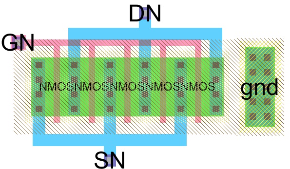
    - 100/2 NMOS (3 pins, DN, GN, SN, connect the p+ body, B, of the NMOS to the chip's ground pin)

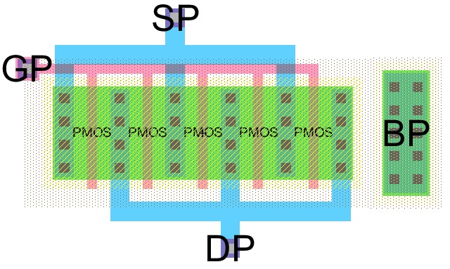
    - 100/2 PMOS (4 pins, DP, GP, SP, and BP)

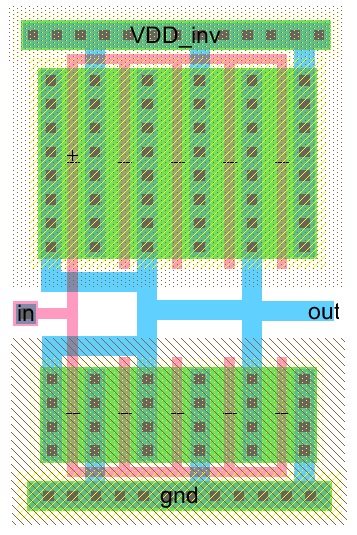
    - Inverter made using 100/2 NMOS and 200/2 PMOS (3 pins, in, out, VDD_inv)

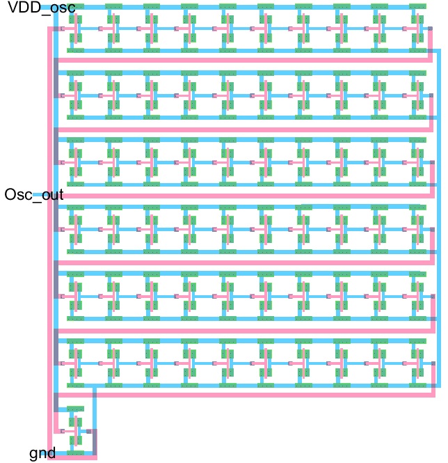
    - 61 stage ring oscillator using 10/2 MOSFETs with off-chip buffer (2 pins, VDD_osc and Ocs_out. Ground connected to pin 20)

    - 20k n-well resistor (2 pins)

    - 20k hi-res poly resistor (2 pins) 

    - 1k n+ resistor (2 pins)

    - 1k p+ resistor (3 pins, need n-well to isolate the p+ from the p-substrate and the n-well needs to be tied to a voltage >= either side of the resistor)

    - Bandgap
 reference (2 pins, VDD_bg and Vref)
- We also added the following to utilize all the space in the pads:
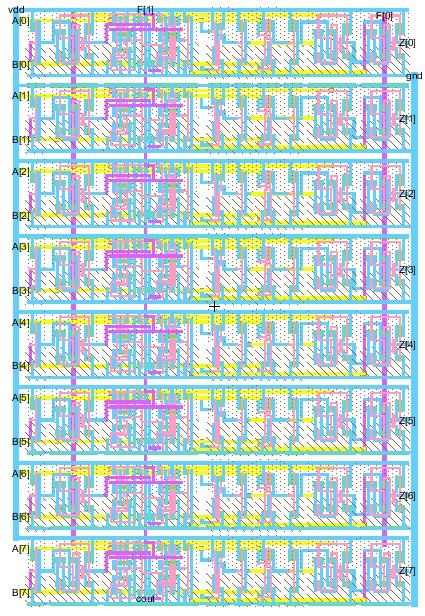
    - 8 Bit ALU from our lab projects
    - XOR gate
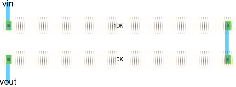
    - Resistive Divider (Divides Voltage by 12)
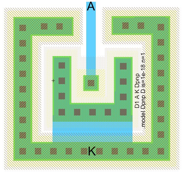
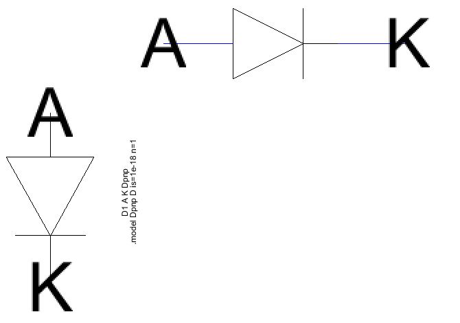
    - Diode Parasitic PNP

 
DOWNLOAD JELIB HERE

 
100/2 NMOS with 3 pins (DN, GN, SN)
Schematic of 100/2 NMOS
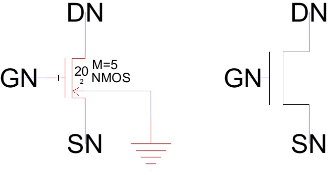
NMOS_schematic.jpg
 
Layout of 100/2 NMOS
NMOS_layout.jpg
 
100/2 PMOS with 4 pins (DP, GP, SP, and BP)
Schematic of 100/2 PMOS
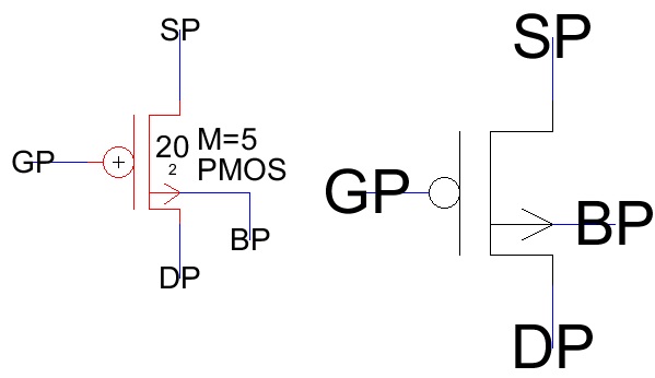
PMOS_schematic.jpg
 
Layout of 100/2 PMOS
PMOS_layout.jpg
 
Inverter made using 100/2 NMOS and 200/2 PMOS with 3 pins (in, out, VDD_inv)
Schematic of Inverter
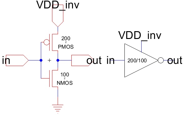
inverter_schematic.jpg
 
Layout of Inverter
inverter_layout.jpg
 
61 stage ring oscillator using 10/2 MOSFETS with off-chip buffer and 2 pins (VDD_osc and Osc_out)
Schematic of ring oscillator
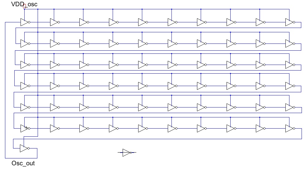
osc_schematic.jpg
 
Layout of ring oscillator
osc_layout.jpg
   
20k n-well resistor with 2 pins
Schematic of 20k n well resistor
n_well_res_schematic.jpg
 
Layout of 20k n well resistor
n_well_res_layout.jpg
 
20k hi-res poly resistor
Schematic of hi-res poly resistor
hi_res_poly_schematic.jpg
 
Layout of hi-res poly resistor
hi_res_poly_layout.jpg  
1k n+ resistor
Schematic of 1k n+ resistor
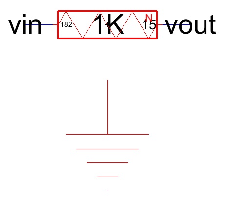
 n_plus_1k_schematic.jpg
   
Layout of 1k n+ resistor
 n_plus_1k_layout.jpg
 
1k p+ resistor
Schematic of 1k p+ resistor
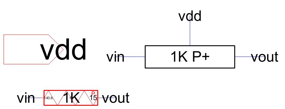
p_plus_1k_schematic.jpg
   
Layout of 1k p+ resistor
p_plus_1k_layout.jpg
   
8 bit ALU with 28 pins (8 pins for A[0:7], 8 pins for B[0:7], 8 pins for Z[0:7], 2 pins for F[0:1], and VDD)
Schematic of 8 bit ALU
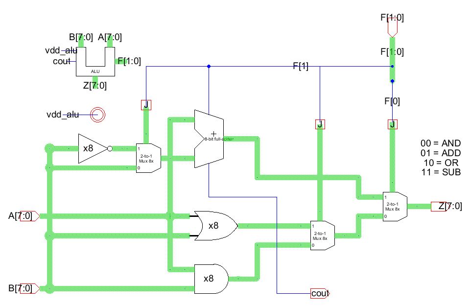
ALU_schematic.jpg
   
Layout of 8 bit ALU
ALU_layout.jpg
 
XOR Gate with 3 pins (A, B, VDD)
Schematic of XOR gate
XOR_schem.JPG 
   
Layout of XOR gate

XOR_layout.JPG 
   
Resistive Divider with 3 pins (Vin, Vout, VDD)
Schematic of
Resistive Divider
R_Divider_schem.JPG
   
Layout of Resistive Divider
R_Divider_layout.JPG
 
Diode Parasitic PNP with 2 pins (K, A)
Schematic of Diode Parasitic PNP
diode_schem.jpg
   
Layout of Diode Parasitic PNP
diode_layout.jpg
 
Overall & Conclusion
Schematic
Final_schem.JPG
 
Layout
Final_layout.JPG
 
 
ALU
vdd = Pin 21
A[0-7] = Pin 22-29
B[0-7} = Pin 30-37
Cout = Pin 38
F[0-1] = Pin 39-40
Z[7-0] = Pin 1-8
gnd = Pin 20
 
PMOS
SP = Pin 23
GP = Pin 24
DP = Pin 25
BP = Pin 26
NMOS
DN = Pin 27
GN = Pin 28
SN = Pin 29
gnd = Pin 20
Inverter
vdd = Pin 19
In = Pin 22
Out = Pin 23
gnd = 20
Bandgap
vdd = Pin 9
Vref
= Pin 1
gnd
= Pin 20
 
XOR Gate
vdd
= Pin 18
 
A = Pin 23
B
= Pin 22
AxorB
= Pin 24
 
R_Divider
vin = Pin 11
vout
= Pin 8
gnd
= Pin 20
Osc
vdd_osc
= Pin 10
osc_out
= Pin 11
gnd
= Pin 20
20k N well
vout = Pin 16
vin 
= Pin 15
20k hi-res
vout
= Pin 16
vin
= Pin 12

1k N+

vout
= Pin 16
vin
= Pin 14
gnd
= Pin 20

1k P+
vout
= Pin 16
vin
= Pin 12
vdd
= Pin 17
Diode
K
= Pin 16
 A = Pin 11


For all testing ground pin 20.
 
To test the ALU, apply
5V to its VDD and the F[1:0] pins to select the desired function.
 
F[1:0] Function
00 AND
01 ADD
10 OR
11 SUB
 
For SUB, Cin must be set to 5V.
Then apply 5V for each pin of the the inputs A[0:7] and B[0:7] and read the result from Z[0:7].
 
To test the PMOS, ground the GP pin and apply voltage to the SP pin, connect the BP pin to SP, and read the output of the DP pin to see how the PMOS turns off as you increase voltage on the GP pin.
 
To test the NMOS, apply 5V to the GN pin and apply voltage the DP pin and read the output of SP pin to see how the NMOS turns off as you decrease the voltage on the GN pin.
 
To test the Inverter, apply 5V to vdd and a varying voltage on In and read the output of Out to see how the inverter inverts the input.
 
To test the bandgap, apply 5V to its VDD, and read the output of Vref which should be a constant 1.25V.
 
To test the XOR gate, apply 5V to its VDD and set each A and B input high or low and read the output AxorB to see how the XOR operation is performed.
 
To test the R_Divider, apply a voltage to Vin and read the output vout which should be 1/12 of Vin.
 
To test the oscillator, apply 5V to vdd_osc and attach osc_out to an oscilloscope to see how the output oscillates while using a DC voltage input.
 
To test the 20K N-well and 20K hi-res resistors, attach an ohmmeter to vin and vout to read the resistance. Alternatively, apply a voltage to vin and vout to read the current (either by the power supply or by connecting an ammeter) and use ohm's law to solve for the resistance which should be 20K. Note all resistors can only be tested one at a time.
 
To test the 1K N+ resistor, test it the same way as the previous resistors while also grounding the gnd pin.
 
To test the 1K P+ resistor, test it the same was as the previous resistors while also applying 5V to the vdd pin.
 
To test the diode, apply a voltage to A and read the voltage at K which should be approximately V(K)-0.7.
 

Return to EE 421L Labs