Lab 6 - EE 421L
Authored
by: Kendrick De La Pena
Date: October 13, 2013
Email: delape19@unlv.nevada.edu
Lab Description
Lab 6 will focus on the design, layout, and simulation of a NAND gate, NOR gate, XOR gate, and a Full Adder.
Lab Work
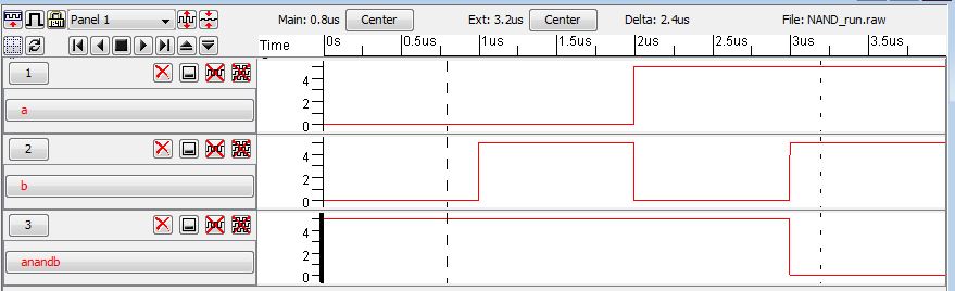
NAND gate
A NAND gate can be made using 2 PMOS devices and 2 NMOS devices. The icon view is at the top of the schematic
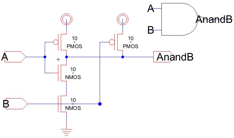
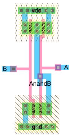
The
layout matches the schematic. A standard cell frame, or an sframe, of
110 was used. The sframe is made larger for more complicated designs. All checks were made with not errors present.
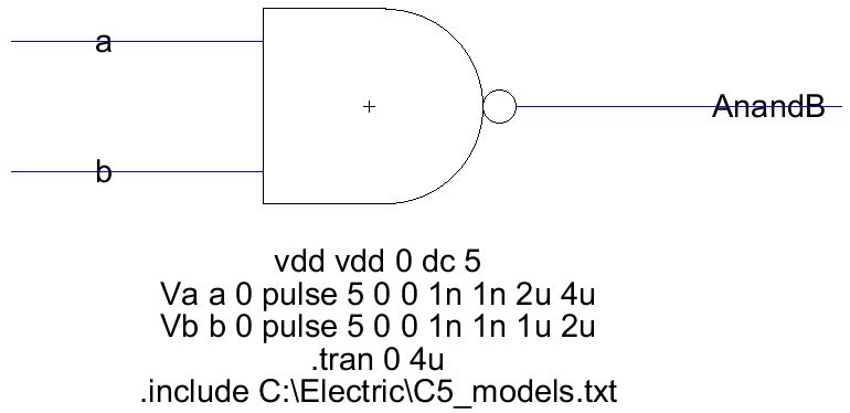
Using
the icon view, a small circuit is created to test the input and output.
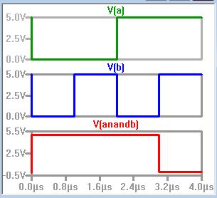
The graph is shown with all possible inputs as well as an IRSIM.
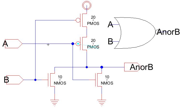
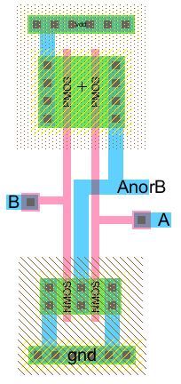
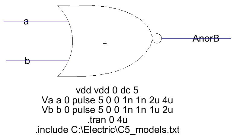
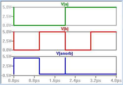
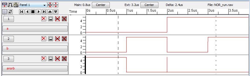
NOR gate
A
NOR gate can be made using the same MOSFETs as a NAND gate but
connected differently. Also, the PMOS devices are 20/2 instead of 10/2.
Layout is as follows. All checks were made.
Schematic and graphs are below
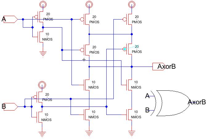
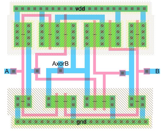
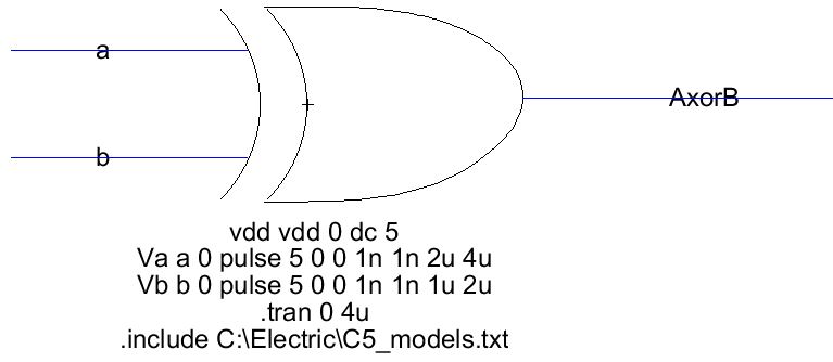
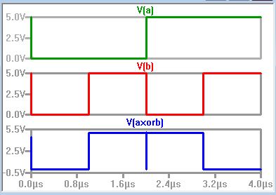
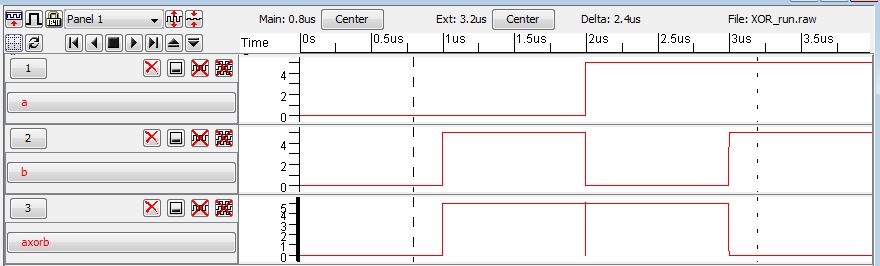
XOR gate
An
XOR gate can be made with four 20/2 PMOS devices and four 10/2 NMOS
devices. However, since the gate requires inverse inputs, two more of
each device are needed, totaling to six PMOS devices and six NMOS
devices.
Layout is as follows. All checks were made.
Schematic and graphs are as follows
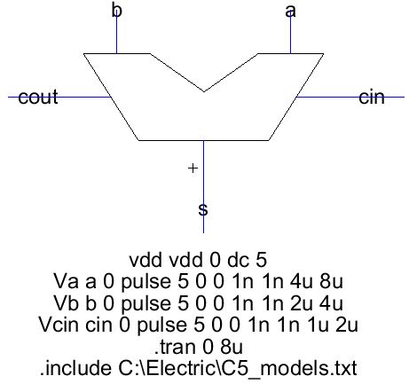
Full Adder
A
full adder can be implemented in two ways. The first way is with three
AND gates, 1 OR gate, and 2 XOR gates. Since we made NAND and NOR
gates, four inverters will be needed to implement the adder in this way.
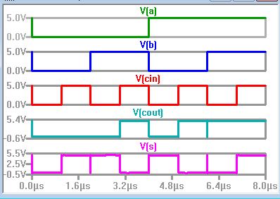
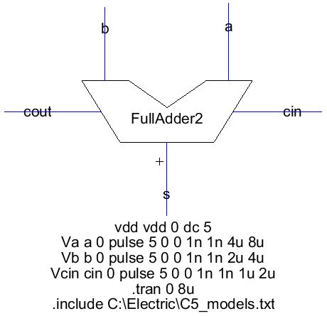
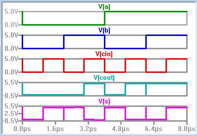
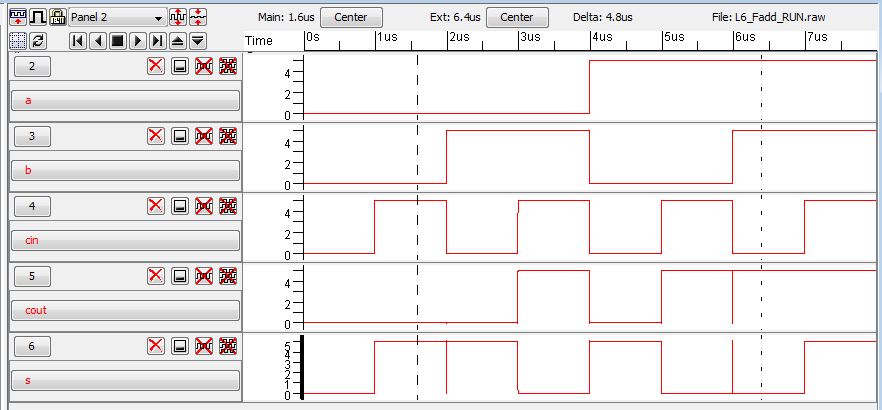
A small circuit is made to show all possible inputs and outputs.
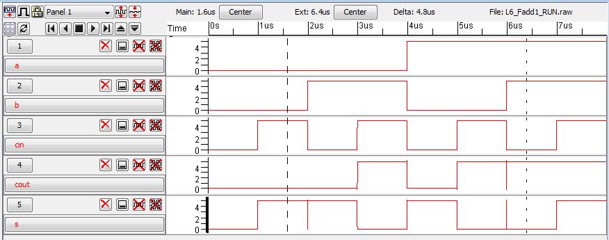
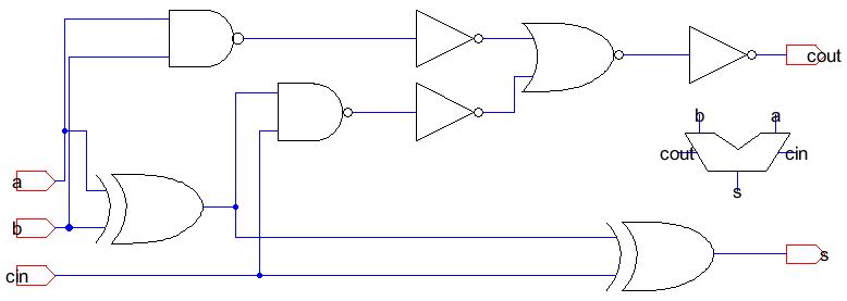
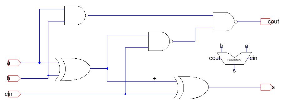
A
full adder can also be implemented with three NAND gates and two XOR
gates. The same steps were taken with the addition of a layout.
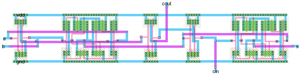
Circuit and graphs are below.
Return to Kendrick's labs