Lab 5 - EE 421L
Authored
by: Kendrick De La Pena
Date: October 4, 2013
Email: delape19@unlv.nevada.edu
Lab Description
Lab 5 will focus on the design, layout, and simulation of a CMOS inverter
Lab Work
1)
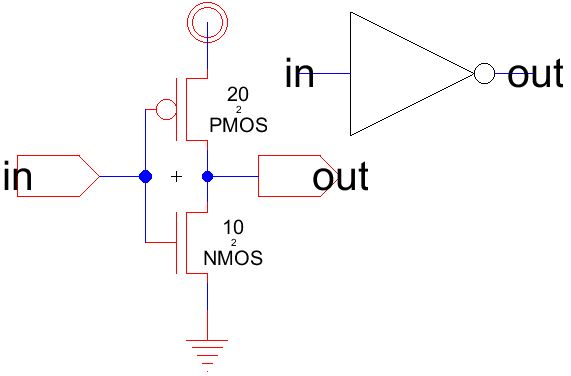
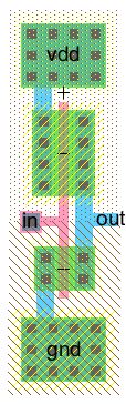
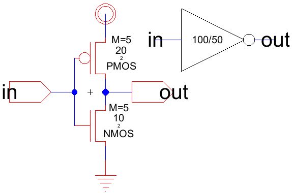
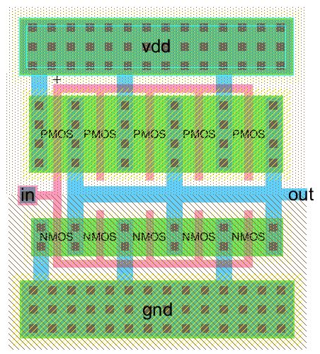
The first step is to create the schematic of the 20/10 inverter using a
20 PMOS and 10 NMOS device as shown below. The layout will follow the
schematic identically. The "in" is connected to poly while the "out" is connected to metal 1. The other connections are shown.
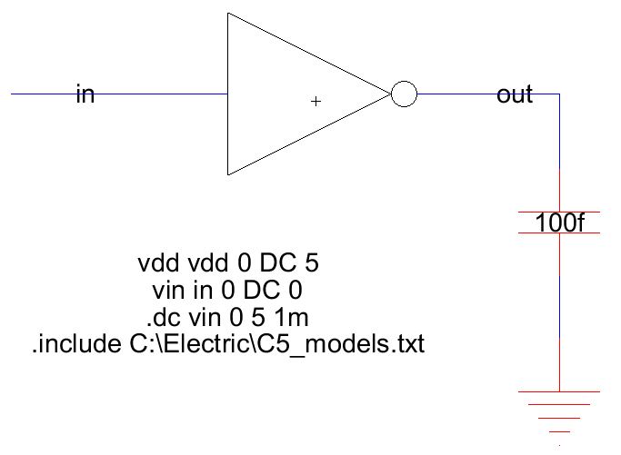
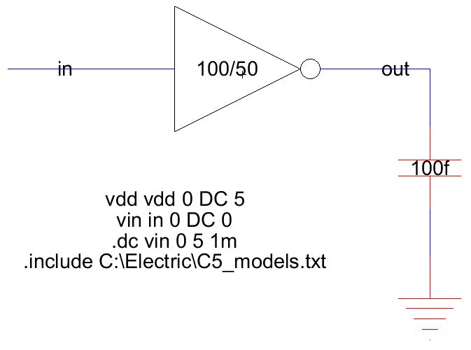
The
next step is to connect a capacitor to the newly created inverter. The
SPICE code used is shown. The capictor is currently at 100 fF, and we
will change the capacitor to 1 pF and 10 pF for additional simulations.
NOTE: Off-page connectors were added for ASL and IRSIM simulations as
they are needed in order to run.
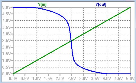
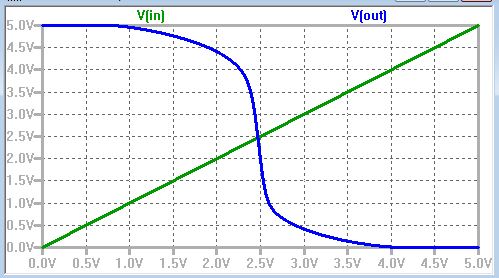
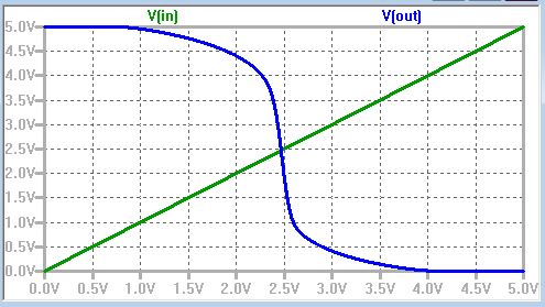
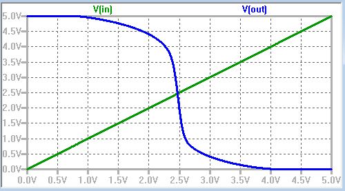
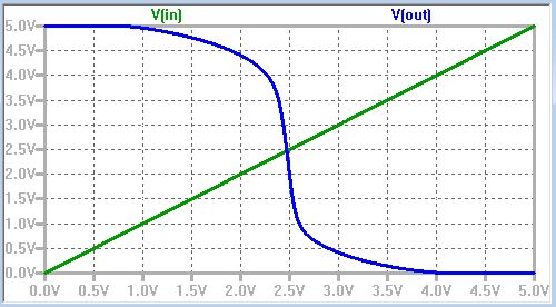
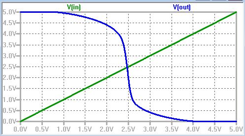
The
simulation results for the inverter driving 100f, 1p, and 10p capacitor
loads are shown from left to right. The graphs are the same since
the capacitor is taken as an open wire. The LT simulation does not
detect any differences
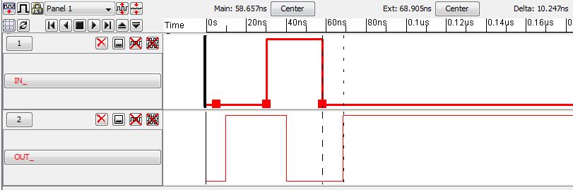
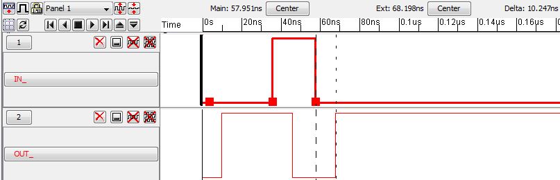
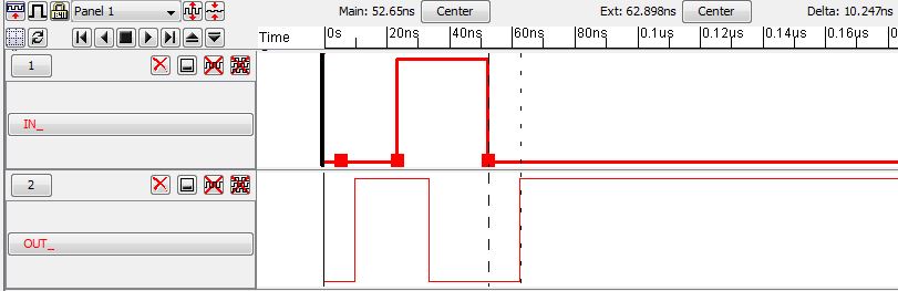
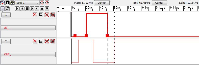
The
ASL simulation results for the CMOS inverter driving 100f, 1p, and 10p
capacitor loads are shown from top to bottom. Similarly to the LTspice
simluations, the ASL simulation does not detect any differences between
the different loads. Delta, or the delay between the input and output,
is roughly 10.2 ns for all loads.
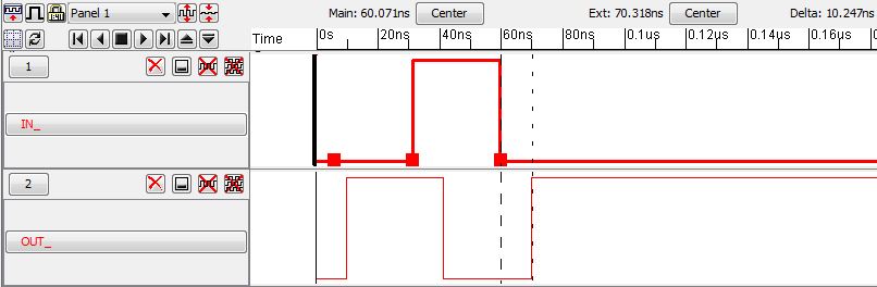
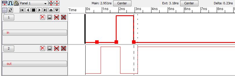
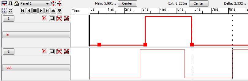
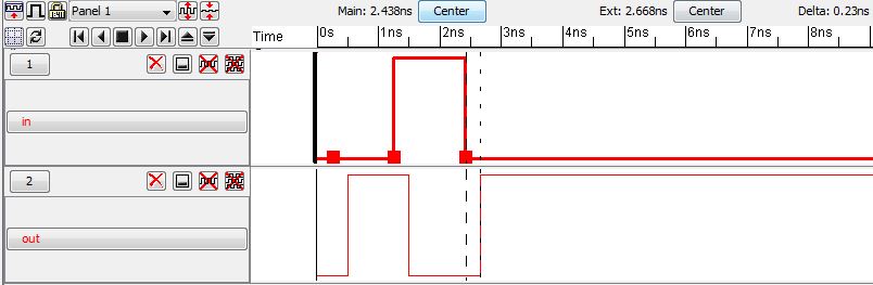
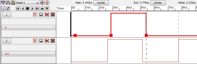
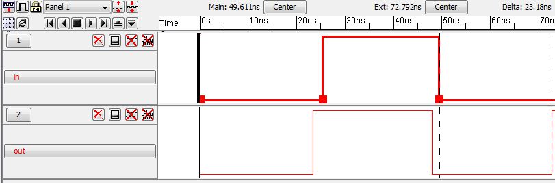
The
IRSIM simulation results for the inverter driving 100f, 1p, and 10p
capacitor loads from top to bottom are shown below. Since the IRSIM
works differently than the previous simulations, the delta, or delay,
increases with higher capacitances. At 100 fF, the delay is 0.23 ns. At
1 pF, the delay is 2.33 ns. At 10 pF, the delay is 23.18 ns.
2)
The above procedures will now apply to a 100/50 CMOS inverter. To
create the schematic, we use a multiplier on the PMOS and NMOS device.
With a multiplier, additional devices will be connected in parallel
automatically. For the layout, the setup is simiiar, but more devices
will be added.
As before, the inveter will drive capacitor values the vary from 100f to 1p to 10p
Since
the ratio are the same (20/10 is equivalent to 100/50), the LT spice
simulation will be the same and show the exact same patterns. The ASL
and IRSIM simulations will also be the same as shown further down.
ASL
simulation results for 100/50 CMOS inverter driving 100f, 1p, and 10p
capacitor loads (top to bottom). Delay is roughly 10.2 ns.

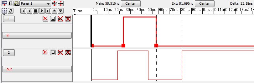
IRSIM
for 20/10 CMOS inverter driving 100f, 1p, and 10p capacitor loads (top
to bottom). Delay values are 0.23 ns for a 100 fF load, 2.33 ns for a 1
pF load, and 23.18 ns for a 10 pF load.
Return to Kendrick's labs