Lab 4 - EE 421L
Email: delape19@unlv.nevada.edu
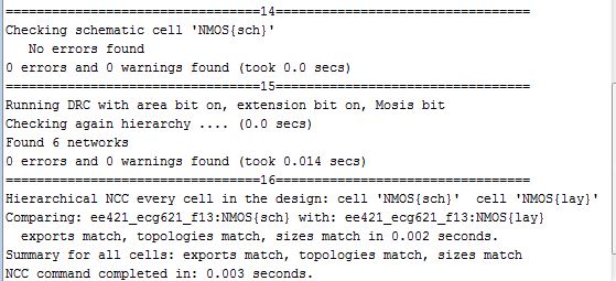
Tutorial 2 was completed as given on the main site.
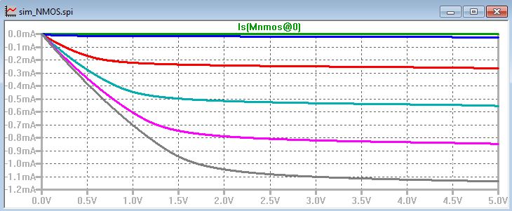
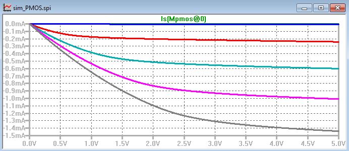
A spice code was used for the simulation. As shown, the source currents for various VGS values went in a negative direction.
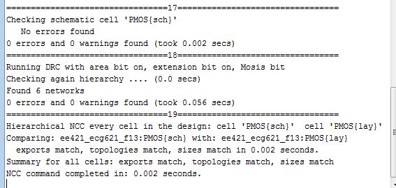
2) In the schematic, a PMOS transistor was used as the body with off-page nodes exported to D, G, and S. A power node was placed to match with vdd in the layout. The layout of the PMOS consists of the PMOS node, 2 pAct nodes, a metal1 to contact to poly 1, and a nWell node for the body connection. The PMOS has characterisitcs of 20/2.
A spice code was used for the simulation. As shown, the source currents for various VGS values went in a negative direction.
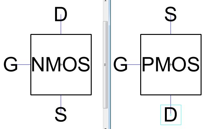
3) In both schematics for NMOS and PMOS, the schematics are in an awkward view. Using the "Make Icon View" in the menu, you can get rid of the floating power/ground, leaving only the connecting wires.