Lab 2 - EE 421L 

Authored by: Kendrick De La Pena

Date: September 5, 2013

Email: delape19@unlv.nevada.edu


Lab Description

Lab 2 will help understand the design of a 10-bit Digital-to-Analog Converter (DAC). The Pre-Lab work will show the following:

  1) Provide narrative of the steps

  2) Provide, and discuss, simulation results different from the above to illustrate your understanding of the ADC and DAC

  3) explain how you determine the least significant bit (LSB, the minumum voltage change on the ADC's input to see a change in the digital code B[9:0]) of the converter. Use simulations to support your understanding.

 
Pre-Lab Work


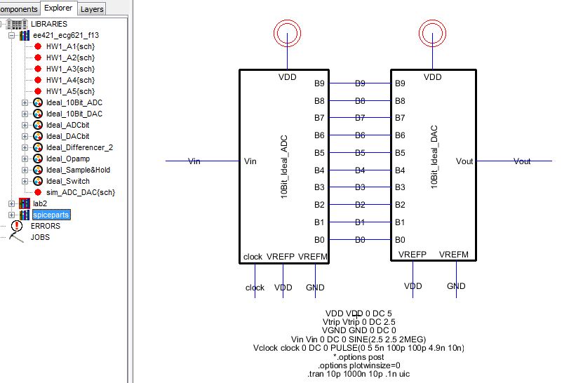
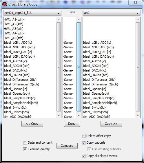
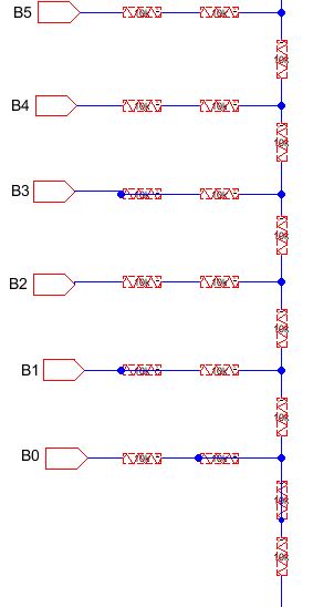
1) After downloading the lab2 library, using the Cross-Library Copy menu command will allow you to obtain the ideal 10-bit ADC and DAC. The following is what your library will look like after the copy.

01%20Cross%20Copy.JPG


2) Select "sim_ADC_DAC(sch)

02%20Select.JPG


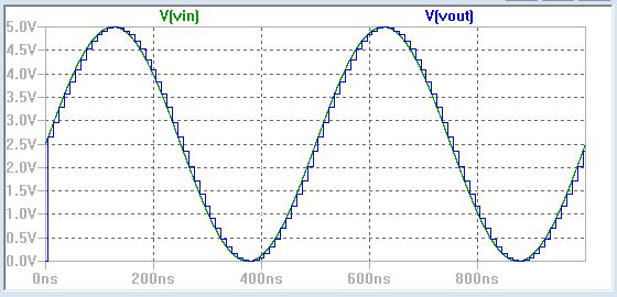
3) Run the simulation and plot the Vin and Vout traces

03%20Sim.JPG

Simulation Results

From the above simulation, the voltage coming appears as a smooth waveform. However, the voltage leaving the device appears as a jagged waveform. This change is the basic operation of a DAC converter.


The least significant bit (LSB) of an ADC's input is the minimum voltage change. LSB can also be defined as smallest change in the DAC's output. The number of bits in the converter, n, determine the LSB through the following equation: VDD over 2 to the power n.
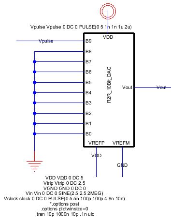
  

Lab Work

1) First, we design a 10-bit DAC using 10k n-well resistors. Resistors are laid out in the following fashion for each pin. Since we are design a 10-bit DAC, we will have 10 pins.

04%20R2R.JPG


Our design, "resistor to resistor" replaces the ideal DAC in the original circuit

04b%20R2R.JPG


The output of the above DAC is the same as the Ideal DAC as shown below

05%20R2R%20Sim.JPG


2) To determine the output resistance, you use repeated series and parallel combinations. Two 10k resistors in series yield a resistance of 20k. Two 20k resistors in parallel yield 10k. The output resistance in general will be R, or in this case, 10k Ohms.

04a%20R2R.JPG


3) Next, we will drive the load by including a 10pF capacitor, connecting a pulse source to the top pin, and grounding the rest.

06%20R2R%20Drive.JPG


In this circuit:

The time delay = 0.7RC = 0.7 * 10e3 * 10e-12 = 70e-9 or 70 nanoseconds.

1 LSB = VDD / 2^n = 5 / 2^10 or  0.977 mV

Since the pulse is connected at the top, the digital code is 10 0000 0000 or 1024.

Vout = Vin/2 or 2.5 V


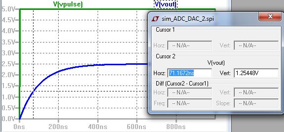
The simulation results are as follows:

07%20R2R%20Drive%20Sim.JPG


4) In a real circuit, transistors (MOSFETs) are used inplace of switched at the outputs of the ADC. Since the resistance of the MOSFETS are not smalll compared to R, the out resisteance is affected, changing the time delay of the circuit as well as the output wave form


Return to Kendrick's labs