
Lab 1 - EE 421L
Email: delape19@unlv.nevada.edu
1) Simply showing the first nine images in this tutorial with some simple narrative.
2) Discussing how you will do regular backups while working on the future labs by zipping up your work and emailing it to yourself (include at least two images to support your discussion).
Lab Report
1) The start up of Electric displays as shown below
2) To change background color to white, go to menu item Window -> Color Schemes -> White Background Colors.

3) Next step is to set up Electric to use ON Semiconductor's C5 Process and fabrication through Mosis.

4) The scale (lambda) must be changed for the C5 process. Go to File -> Preferences -> Technology -> Scale and set mocmos scale to 300 nm.
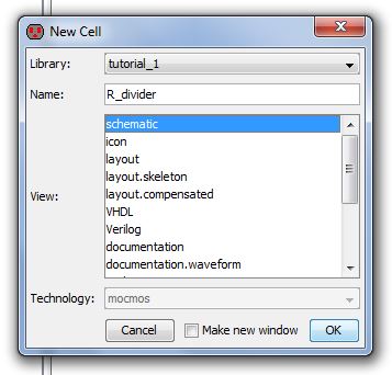
5) Next step is to draw the schematic of a resistive divider. Go to Cell -> New Cell and enter the cell name (R_divider) and view (schematic).

7) In the Component menu, there is a box containing a resistor and the word “Normal.” Select N-Well version with the arrowhead and place it into the schematic.

8) Change the properties by clicking that node and going to the object properties. Use the settings as shown below.

9) The edited resistor will display as shown.

Backup
Backups will made save through the Dropbox application. A copy is saved on my hard drive as well as on the internet.

