Lab 7 - EE 421L
Authored
by Chad Johnson,
ctjohnso@unlv.nevada.edu
10/18/2013
In
this lab I will explore arrays, busses, and I will layout an 8-bit
adder. Array and bus functionality allows easily created, easily
readable, concise schematics. Creating of the 8-bit full adder will be
the most complex layout I have constructed yet. It will require a neat
and organized approach. Also, I will create a 2 to 1 demux and an 8-bit
2 to 1 demux in preparation for the ALU unit to be completed for the
final project.
I begin by completing tutorial 5, which explored ring oscillators, buses, and arrays. Shown below is the parallel inverts completed in the tutorial.

Also completed in the tutorial was a series of inverters in series, functioning as a ring oscillator.

The
ring oscillator was also layed out to demonstrate the NCC comparison
between the schematic's arrays and busses and a layout.

After
completeting the tutorial, I started into the lab. First I created 8
inverters in parallel as shown in the schematic below.

The
functionality of the schematic was demonstrated in the simulation shown
below. Note that the outputs drive different capacitive loads, and that
the inverter does not function very well with large capacitive loads.

The simulation results are shown below.

Next
I turn my attention to making 8 bit arrays of other gates. Shown below
is an 8 bit NAND gate array, 8-bit NOR gate array, 8-bit AND gate
array, and an 8-bit OR gate array.


These gates were simulated together. Their functionality is demonstrated in the Spice simulations shown below.


Next I progressed into creating a 2 to 1 demux, shown below.

The functionality of the circuit is shown below. The Spice Simulation demonstrates the correct functionality of the demux.

The
demux circuit can function as a MUX. In the simulation below, a source
is applied to the Z node to show that it can function as a 2 to 1 MUX.


Now
it was time to array the 2 to 1 demuxs that are controlled by a single
input. The schematic of the 8 bit demux circuit is shown below.

The spice simulation circuit is as follows.

The results show the correct operation of the demux.
This circuit was also simulated in the circuit shown below. Note that the IRsim demonstrates the summation of A, B, and C.

Lastly,
I began to take steps to the completion of a layout for an 8-bit full
adder. I begin by created a full adder schematic shown below.

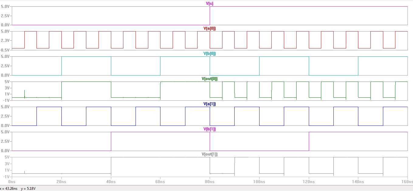
The schematic was simulated by IRsim.

Next, this circuit was used in the creation of an array schematic for an 8-bit full adder schematic.

The
functionality of this circuit was also simulated in IRsim, note that
the bus lines show a hexadecmial number to display the status of the
buses.

Next
the 8-bit full adder was layed out. I began by laying a 1-bit full
adder and NCCing it with the 1-bit full adder schematic. This can be
confirmed in the library file found in this directory.
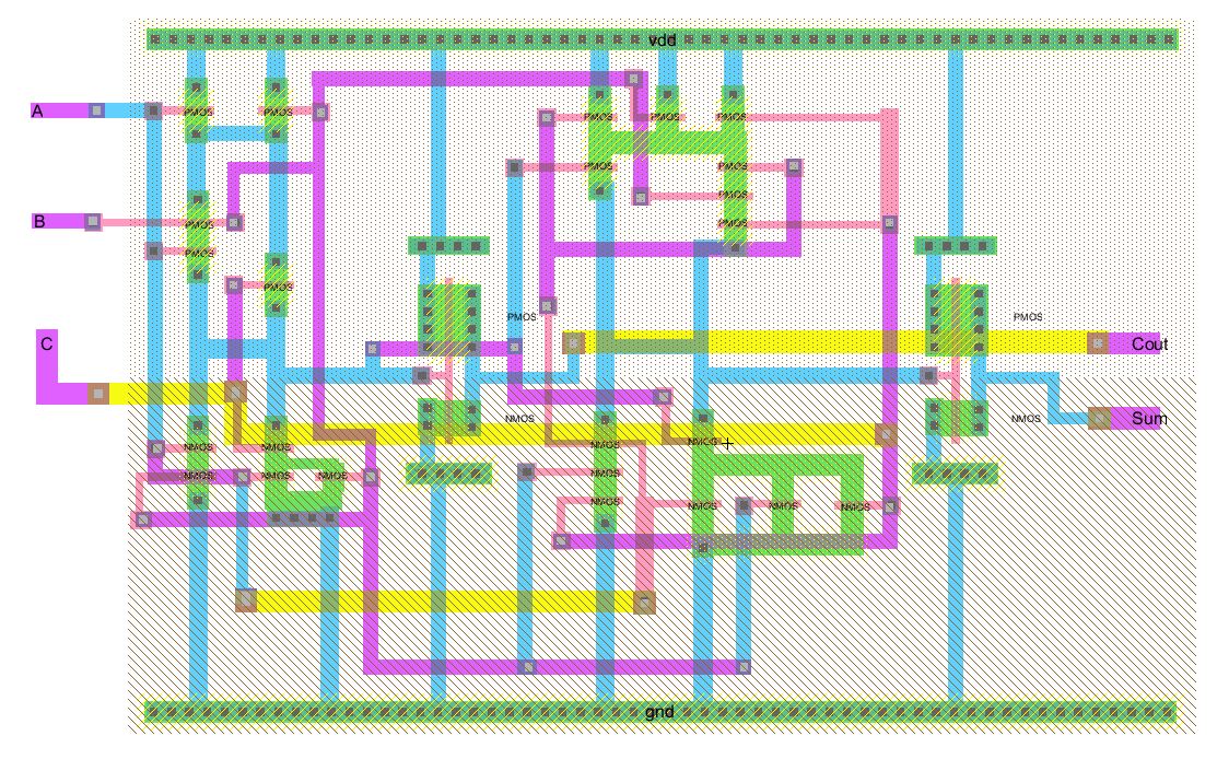
Shown below is the 8-bit full adder along with its DRC, Well Checks, and NCC checks.


This completes lab 7. Lastly I back up all my work as shown below.

Lab7 jelib is found here.
Return to Chad Johnson's EE 421 Lab Reports