Lab 6 - EE 421L
Authored
by Chad Johnson,
ctjohnso@unlv.nevada.edu
10/11/2013
In
this lab we will create schematics, layouts, and simulate the
operations of NOR gates, XOR gates, and NAND gates. Then, using these
components, we will create a layout, schematic, and simulate the
operation of a full adder.
I
begin by completing the tutorial, which had me create the NAND gate.
Upon starting the lab I notice that the first portion of the lab is to
create a NAND gate with 10/2 pmos and 10/2 nmos. The icon for this is shown below.

The schematic for the NAND gate is shown below.

The DRC and NCC for the schematic is shown below.

We note that this design is similar to the tutorial except for the sizing of the pmos. The layout is shown below.

The DRC, Well Check, and NCC for the layout is shown below.

The design was simulated in Spice to show operation. Note that the
pulse show all possible input combinations. Shown below is the
simulation schematic and the results.


Next the same procedure was done constructing a NOR gate. First the schematic and icon for the NOR gate were constructed.


The DRC and NCC for the 2 input NOR schematic are shown below.

The corresponding layout for the 2 input nor gate is shown below.

The DRC, Well Check, and NCC for the 2 Input NOR were successful as shown below.

Next the 2 input NOR gate was simulated in Spice to confirm functionality. The simulation circuit and results are shown below.


Next
the 2 input NOR gate was simulated with IRsim, which is a logic
simulator that considers the delays of the transistors. The IRsim
simulation schematic and results are shown below.


Next,
as was done for the 2 input NAND and 2 input NOR gates, a 2 input XOR
gate was created. The icon and schematic for the 2 input XOR gate are
shown below.


The DRC and NCC for the 2 input NOR schematic is shown below.

The corresponding 2 input xor gate is shown below.

The DRC, Well Check, and NCC for this are shown below.

The functionality of the XOR gate was simulated first in Spice. Shown below is the simulation schematic and results.


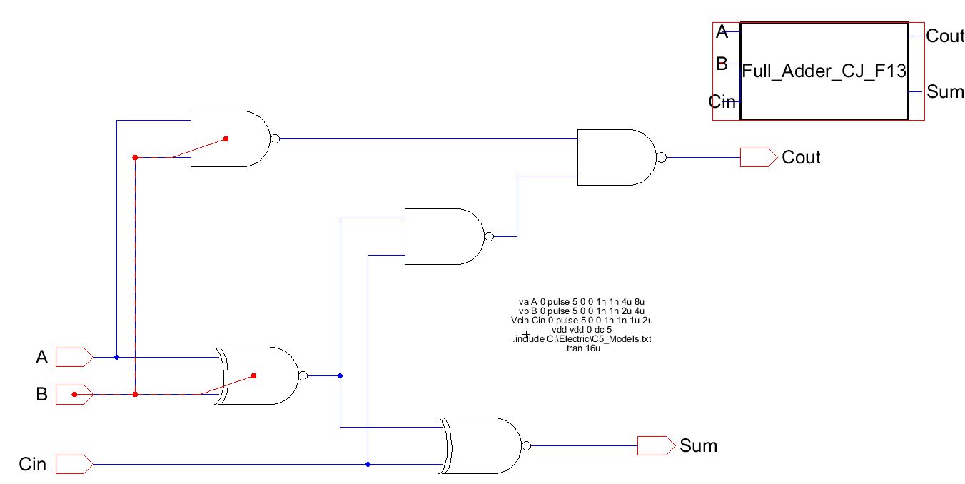
Lastly, the above gates were used in the construction of a full
adder. The icon and schematic for the full adder are shown below.

The layout of the full adder was as follows.

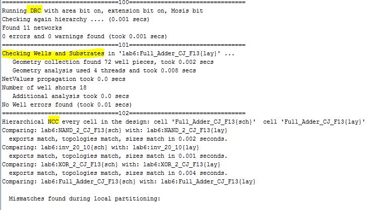
The
DRC, Well Check, and NCC are shown below. Note I was unable to get the
schematic to NCC correctly even though both the schematic and the
layout simulate correctly in spice.
Note
the spice commands in the above schematic. The simulation results are
as shown below. They confirm the correct functionality of the full
adder.


We note discrepancy with the IRsimulation despite the fact that the Spice simulation shows correct functionality.
Lab6 jelib is found here.
Return to Chad Johnson's EE 421 Lab Reports