Lab 4 - EE 421L
Authored
by Chad Johnson,
ctjohnso@unlv.nevada.edu
9/27/13
In
this lab we will create layouts and schematics for PMOS and NMOS
transistors of different sizes. Also we will simulate our layouts and
schematics to obtain the IV characteristics.
We
begin by completing the MOSFETS in the tutorial. From this point we
will create MOSFETS to be simulated for the lab. We will also discuss
how to create a cell icon.
The construction
of the PMOS is detailed below. Construction of the NMOS was similar.
First we add a PMOS (poly over active, where the poly will funciton as
the gate), 2 pActive connections (for source and drain), and a Nwell
connection (for connection to VDD). This is shown below.

We used the multi-object properties tool to adjust these widths at the same time.
The
desired width for the PMOS is 20, Thus each element (except for the
poly connection) is resized to a width of 20. Note that the length of
the nwell connection (which will be connected to VDD) is also adjusted
to have a length of 6.

Next, the gate, drain, and source are connected as shown below.

The
connections to the gate and drain are then moved in to a tighter form,
and the VDD connection is moved to have contact with the nwell of the
other parts.
The
desired width for the PMOS is 20, Thus each element (except for the
poly connection) is resized to a width of 20. Note that the length of
the nwell connection (which will be connected to VDD) is also adjusted
to have a length of 6.
Lastly, connections are made to metal 1 from the gate, drain, source,
and bulk. These metal connections are exported with their respective
names. And, as indicated in the lab, the name of the PMOS is changed to
reflect my initials. The final result is shown below.

The NMOS was simulated as shown below.
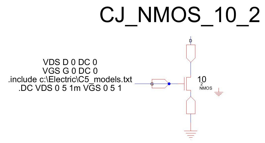
The corresponding layout for this schematic is as shown below.

The simulation results for the nmos are as follows.
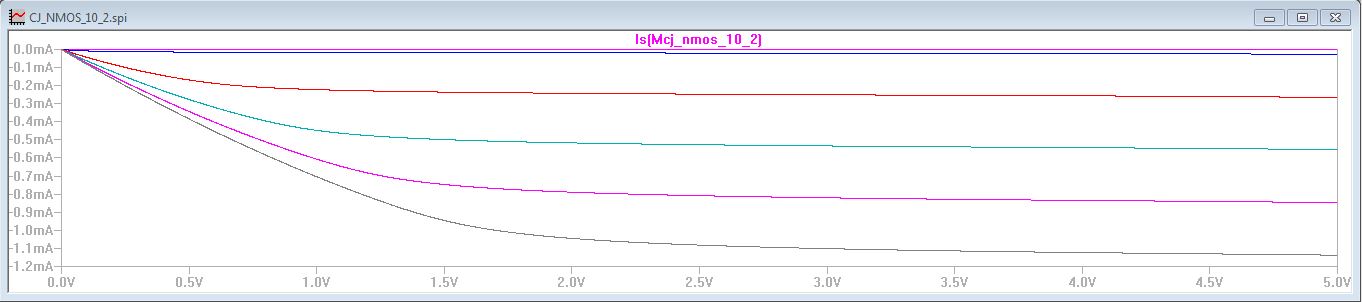
Note
that I selected source current and I could have very well selected
drain current or perhaps changed the orientation of the current,
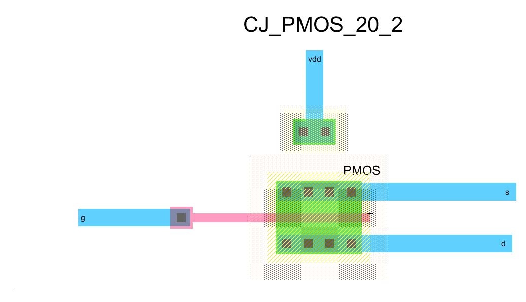
The completed PMOS was simulated as shown below.
The corresponding layout for this schematic is as follows.
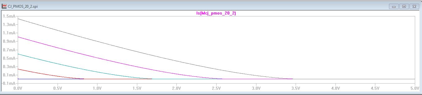
The simulation for this cell is shown below.
My lab information was zipped up and backed up in my dropbox folder as shown below.

Return to Chad Johnson's EE 421 Lab Reports