Lab 3 - EE 421L
Authored
by Chad Johnson,
ctjohnso@unlv.nevada.edu
9 13 2013
In
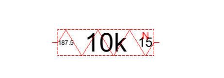
this lab we will layout the 10-bit digital to analog converter that we
drew the schematic for in lab 2. A small variation of the resistor form
tutorial 1 was used. The desired resistance value is 10k. We can
compute the value of the resistor as a function of the dimensions of
length, width, and the sheet resistance of the process. Namely
Resistance = Sheet Resistance * (Length / Width). We look up the
information from the MOSIS C5 process and discover that the sheet
resistance is 800 ohms. It is determined that suitable dimensions are a
length of 187.5 and a width of 15. However, this measurement excludes
the region immediatly surrounding the metal contact. Thus the
resistance calculation is not including a small portion of the nwell,
and therefore our computer resistance might be over the target. This
might suggest that we select a length of 180 instead of 187.5. Also, we
note that this number is well within the tolerances of the sheet
resistance. In order to layout our non ideal 10-bit digital to analog
converter we first layout a single cell with the resistor dimensions
listed above.
Shown below is the resistor created from tutorial 1.
Shown below is the schematic and layouts of individual
cells used in the construction.
Schematic:

Schematic Icon:

Layout:

As
previously stated, 10 of these cells are strung together to create the
10-bit DAC. The schematics and layout versions of these are shown below.
Schematic:

Layout:

DRC, NCC, and ERC checks are shown below.


My work is backed up as shown below.

Lab3 jelib file is found here.
Return to Chad Johnson's EE 421 Lab Reports