

Lab 6 - ECE 421L
Design, layout, and simulation of CMOS NAND/NOR/XOR gates and a full-adder
Pre-Lab: Go through tutorial4 and Electric video 11 before the lab. Lab will make heavy use of the tutorials.
Design 1- NAND Gate
Follow
tutorial 4 and design both layout and schematics of a NAND
gate using MOSFETS. Duplicate the tutorial NAND gate for this lab,
changing the PMOS to W=10 L=2, naming the cells NAND_NAME_SEMESTER; ie:
NAND_KEN_F13.{schm}/.{lay}.
We should have the following layout and schematics:
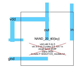
To simulate the device, create a new cell called NAND_SIM and connect it as follows. Simulate the results


Simulate the layout as well:
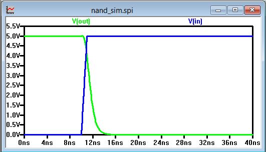
Next, test logic of the NAND gate for all possible inputs using LTSpice and IRSIM:


Design 2 - NOR Gate
Look up the transistor-level design of a NOR gate and construct the design by copy/pasting the transistors from the NAND design. Change the PMOS W to 20.
Similearly, we can just re-wire the NAND layout design to form the NOR layout design. Make sure to change PMOS width to 20 and DRC/Well Check/ LVS.


To simulate the device, create a new cell called NOR_SIM and connect it as follows. Simulate the results.


Simulate the layout as well:

Next, test logic of the NAND gate for all possible inputs using LTSpice and IRSIM:


Design 3 - XOR Gate
Look up the topology of an XOR gate. Using the MOSFETs from the previous design, layout the XOR. You can use the inverter from lab 5. Make sure the size of the PMOS are 20/10 and do not change the NMOS.

The layout for the XOR gate is much more complex; however, only involves copy/pasting MOSFETs into a standard cell frame.
Next, we need to simulate the design. Create a new cell called XOR_SIM and simulate the following:


Next, simulate the logic of the XOR gate in LTspice and IRSIM


There are glitches on the output from the switching inverter.
Design 4 - Full Adder
We have designed all the components needed for a full adder. Lets connect them and make an icon view:


Next, we can design a second full adder using a different topology:

Next, we simulate the full adder again:


Finally, we back up are files:
