reedj35@unlv.nevada.edu
- Experimentally
generate, for the NMOS device, plots of:
1.
ID v. VGS (0 < VGS < 3 V) with VDS = 3 V
2.
ID v. VDS (0 < VDS < 5 V) for VGS varying from 1 to 5 V in 1
V steps, and
3.
ID v. VGS (0 < VGS < 5 V) with VDS = 5 V for VSB varying
from 0 to 3 V in 1 V steps.
- Note that for this
last one, if VSS (NMOS body) is ground (again, the Body, VB, is
grounded) then the source voltage will be varied from 0 to 3 V in 1 V
steps to realize VSB ( = VS - VB = VS) varying from 0 to 3 V in 1 V steps.
At the same time VGS will be varied from 0 to 3 V (when VS = 0), 1 to 4 V
(when VS = 1 V), 2 to 5 V (when VS = 2 V), and 3 to 5 V (when VS = 3
V). In other words, as VS is increased by 1 V the VGS has
to shift up by 1 V as well.
- Assuming that the
length of the NMOS is 5 um and its width is 500 um calculate
the oxide thickness if Cox (= C'ox*W*L) = 5 pF.
- From this measured
data create a Level = 1 MOSFET model with (only) parameters: VTO, GAMMA,
KP, LAMBDA, and TOX.
- Compare the
experimentally measured data above (the 3 plots) to LTspice-generated
data (again, 3 plots) and adjust your model accordingly to get better
matching.
- Experimentally,
similar to what is seen on the datasheet (AC test circuits seen on page 3
of the datasheet), measure the delay of an inverter using these devices
(remember the loading of the scope probe is around 15 pF and there is
other stray capacitance, say another 10 pF).
- Using your model
simulate the delay of the inverter and compare to measured results. Adjust
your SPICE model to get better matching between the experimental data and
the measured data.
- Repeat the above
steps for the PMOS device where VDS, VGS, and VSB are replaced with VSD,
VSG, and VBS respectively.
Experiment
1: NMOS

Figure 1: Pinout diagram for CD4007
For this
experiment, we used the NMOS from pins 6, 7, and 8 to make measurements and
generate the plots from above. We applied the voltages appropriately and then
measured the drain current using the multimeter being in series with the drain
of the MOSFET and the voltage source.
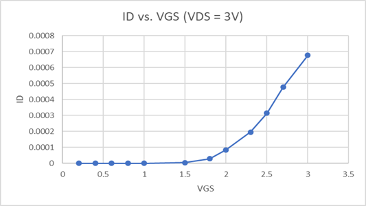
ID v. VGS (0 < VGS < 3 V) with VDS = 3 V
|
Figure 2: Circuit used to simulate
sweeping VGS where VDS = 3V |
Figure 3: Experimentally generated
plot for ID vs. VGS and VDS = 3V |
Figure 4: Plot of ID vs. VGS using
Level=1 model parameters |
ID v. VDS (0 < VDS < 5 V) for
VGS varying from 1 to 5 V in 1 V steps
|
Figure 5: Circuit used to simulate
sweeping VDS and varying VGS *NOTE*: With VGS = 1V and sweeping VDS, ID = 0 all across |
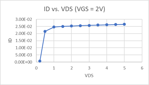
Figure 6: ID vs. VDS as VDS is swept
and VGS = 2V |
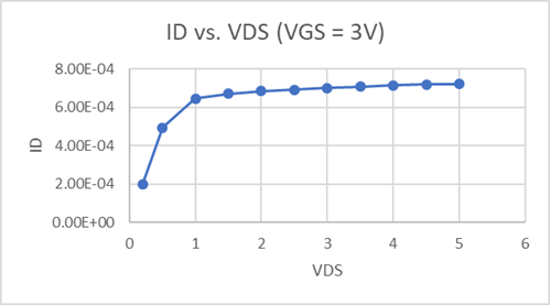
Figure 7: ID vs. VDS as VDS is swept
and VGS = 3V |
|
Figure 8: ID vs. VDS as VDS is swept
and VGS = 4V |
Figure 9: ID vs. VDS as VDS is swept
and VGS = 5V |
Figure 10: Plot of ID vs. VDS using
Level=1 parameters |
For figure 6 above, I believe there
may have been an error with how we were measuring the current or how we had the
circuit set up. The current is much
higher than it should be. This was
not realized until after it was too late to try and revisit the circuit. The
other plots (figures 7, 8, and 9) agree much better.
ID v. VGS (0 < VGS < 5 V)
with VDS = 5 V for VSB varying from 0 to 3 V in 1 V steps
|
Figure 11: Circuit used to simulate
sweeping VGS and varying VSB |
Figure 12: ID vs. VGS as VGS is swept
and VSB = 0V and VDS = 5V |
Figure 13: ID vs. VGS as VGS is swept
and VSB = 1V and VDS = 5V |
|
Figure 14: ID vs. VGS as VGS is swept
and VSB = 2V and VDS = 5V |
Figure 15: ID vs. VGS as VGS is swept
and VSB = 3V and VDS = 5V |
Figure 16: Plot of ID vs. VGS using
Level=1 parameters |
The simulation plots for this
circuit seem to be similar in shape, however, the values are far off from one
another. I will update the model text file
and show an updated version below.
Experiment
2: PMOS

Figure 17: Pinout for CD4007
For this
experiment, we used the PMOS from pins 1, 2, and 3 to make measurements and
generate the plots from above. We applied the voltages appropriately and then
measured the drain current using the multimeter being in series with the drain
of the MOSFET.
ID v. VSG (0 < VSG < 3 V) with VSD = 3 V
|
Figure 18: Circuit used to simulate
sweeping VSG and VSD = 3V |
Figure 19: ID vs. VSG |
Figure 20: Plot of ID vs. VSG using
Level=1 parameters |
ID v. VSD (0 < VSD < 5 V) for
VSG varying from 1 to 5 V in 1 V steps
|
Figure 21: Circuit used to simulate sweeping VSD and varying VSG *NOTE*: With VSG = 1V and sweeping VSD, ID = 0 all across |
Figure 22: ID vs. VSD where VSG = 2V |
Figure 23: ID vs. VSD where VSG = 3V |
|
Figure 24: ID vs. VSD where VSG = 4V |
Figure 25: ID vs. VSD where VSG = 5V |
Figure 26: Plot of ID vs. VSD using
Level=1 parameters |
For this
one, obviously the threshold voltage is set too high in the model parameters
since there is no current for both VSG = 1V and 2V.
ID v. VSG
(0 < VSG < 5 V) with VSD = 5 V for VBS varying from 0 to 3 V in 1 V steps
|
Figure 27: Circuit used to simulate
sweeping VSG and varying VBS where VSD = 5V |
Figure 28: ID vs. VSG where VBS = 0V
and VSD = 5V |
Figure 29: ID vs. VSG where VBS = 1V
and VSD = 5V |
|
Figure 30: ID vs. VSG where VBS = 2V
and VSD = 5V |
Figure 31: ID vs. VSG where VBS = 3V
and VSD = 5V |
Figure 32: Plot of ID vs. VSG using
Level=1 parameters |
Experiment 3
For this experiment,
we will be using the plots from above to create a Level=1 model of both the
NMOS and PMOS used from the CD4007. We will be using this model
to simulate
the MOSFETs in LTSpice and compare the simulations to
the experimentally generated plots. The parameters to be calculated are: VTO, TOX, KP,
LAMBDA, and GAMMA.
VTO:
To find VTO, we just need to look at figures 3 and 19. Figure 3
will help us estimate the threshold voltage of the NMOS by drawing a line along
the slope of the plot where
it becomes linear. The value for VGS as it intersects with the
x-axis will tell us the threshold voltage. The same holds for the PMOS.
Knowing the above, ![]()
TOX:
To calculate TOX, we find in the textbook that ![]() where
where ![]() .
.
We also know, ![]()
We can now solve for TOX: 
KP:
To calculate KP, we must look at figures 3 and 19 again. Looking
at a voltage that is above
VTO, find its corresponding ID value and then using the square-law equation,
we can solve for KP. In doing so, we see that when VGS = 3V,
IDN = 678µA and when VSG = 3V, IDP = 276µA.
Solving for KP we get: ![]()

LAMBDA:
To find lambda for both NMOS and PMOS, we must look at the
experimentally generated plots for the ID vs. VDS @ VGS = 3V and ID vs. VSD @
VSG = 3V, respectively.
The corresponding plots are figures 7 and 23. Find the slope in
the saturation region (finding ID at VDS/VSD = 3V and 2.5, subtracting them and
dividing by 0.5V) and dividing
the slope by ID,sat
which can be found by finding out what the ID is at the threshold voltage for
each device.

GAMMA:
To find gamma, we turn to the textbook and find 


Figure 33: CD4007 Level=1 Model Parameters
The parameters above were used for the plots above. After examining
the discrepancies, I updated the model parameters text file which is seen
below.
NMOS:
|
Figure 34: CD4007 Model Parameters to
improve matching |
Figure 35: ID vs. VGS with VDS = 5V
and VSB varying |
Figure 36: Improved ID vs. VGS with
VDS = 5V and VSB varying |
The biggest disparity for the NMOS experiment was ID vs. VGS with VDS
= 5V and varying VSB from 0V to 3V. The screenshot in the middle is from the
original
model parameters, and the screenshot on the right is the updated
plot.
PMOS:
|
Figure 37: CD4007 Model Parameters to
improve matching |
Figure 38: ID vs. VSD for VSG varying
from 1V to 5V |
Figure 39: Improved ID vs. VSD for
VSG varying from 1V to 5V |
|
|
Figure 40: ID vs. VSG where VSD = 5V
and VBS varying |
Figure 41: Improved ID vs. VSG where
VSD = 5V and VBS varying |
The biggest disparities for the PMOS experiment was ID vs. VSD for
VSG varying from 1V to 5V, and ID vs. VSG where VSD = 5V and VBS varied from 0V
to 3V.
The screenshots in the middle are from the original model
parameters, and the screenshots on the right are the updated plots.
Experiment
4: Inverter Delay
For this experiment, we will be using one of the AC test circuits
from the CD4007 datasheet. Below are figures of the test circuit I am using and
the method of measurement of the delay.
|
Figure 42: AC Test Circuit from
CD4007 Datasheet |
Figure 43: Switching Waveform (to
calculate propagation delay) |

Figure 44: Experimental measurement of
propagation delay from high to low
From figure 44, we can see that ![]()
|
Figure 45: Original CD4007 Model
Parameters |
Figure 46: AC Test Circuit in LTSpice |
Figure 47: Resulting measurement of
propagation delay |
We can see from figure 47 that the propagation delay is the
difference of the two measurements ![]() .
.
The matching is reasonable, and the parameters should not have to
be changed to improve matching.
I will, however, see what the delay is with the improved model
parameters used above.
|
Figure 48: Improved CD4007 Model
Parameters |
Figure 49: AC Test Circuit in LTSpice using improved model parameters |
Figure 50: Measurement of delay |
From figure 50, the delay is ![]() The improved model parameters made the
simulated delay further off from the experimental measurement.
The improved model parameters made the
simulated delay further off from the experimental measurement.
I believe that this is due to the change that I made to lambda.


