Lab 9 - EE 420
Author: Nicholas Mingura
E-mail: mingura@unlv.nevada.edu
4/24/2019
Lab
description:
In this lab you may need to use two,
or more, CD4007 chips from the same production lot (see date code on
the top of chip) to ensure using a BMR to bias a current mirror is
possible. If the CD4007 chips are not from the same production lot they
will not "match" so current mirrors will not be possible.
- Build your BMR design and characterize it as you did in the pre-lab (if you use two chips ensure that grounds and VDDs of both chips are tied together).
- You
expect the BMR to become unstable if there is a large capacitance
across the resistor, such as a scope probe (important), so care must be
exercised
- Use your BMR to bias, and thus create, a:
- NMOS current mirror
- PMOS current mirror
- Measure how the current varies through each current mirror as the voltage across the mirror changes.
- Of
course the current in the NMOS (PMOS) current mirror goes to zero as
the voltage on the drain of the output device moves towards ground (VDD)
- Using these current mirrors drive two gate-drain connected transistors
- For the first experiment use the NMOS current mirror to drive two PMOS gate-drain connected devices.
- Use
the voltages on the gate-drain connection of the two devices to bias a
cascode current mirror (characterize this mirror as before)
- For the second experiment switch, that is, use the PMOS current mirror to drive two NMOS gate-drain connected devices.
- Again, use these two voltages to bias an NMOS cascode current mirror then characterize.
Lab:
For the lab studnets were given the following BMR circuit and to choose a resistor value for R1 based on chips.

Image 1: Given BMR circuit.
While
the above process shows that the 50k resistor was the value calculated
for the chip, the values through out the lab were not what was
expected. This could be due to a mischaracterizationof the chip from
the previous lab, giving differnt values for the parameters that were
used for calculating the resistor. For the experiments the following
points were measured for our values:
Vbiasn ( M3 gate), Vbiasp (M2 gate), and the voltage across the
resistor to obtain Iref. Originally the multimeter was going to be put
in series with the resistor to get the current, but the current was so
low that the multimeter was unable to read the current, however the
voltage was large enough for the multimeter to read. Then the voltage
was divided by the resistance to get the current.
After
getting the table the values were put into excel plots to see how the
plots looked. To the right of each of the excel plots is an LTSpice
simulation of the same circuit to see if they are working as
expected.


Image 3: Vbiasn plot for the BMR circuit.


Image 4: Vbiasp plot for the BMR circuit.
From
the simulations and the experimental values it can be seen that the
voltages in the biasp is nearly the graph, however the vbiasn does not
flatten at the same point. This could be that resistor value was chosen
incorrectly, however the equations above still seem to be true.
Additionally the LTSpice models were made characterizing one chip but
these lab required two chips, it is possible that the chips are
slightly differnt so the values will be slightly off.
After
creating the BMR circuit it was tested with both a nmos and pmos
current mirror showing the current going through each of them.


Image 6: Nmos (Left) and Pmos (Right) current mirrors with BMR circuit.
After getting the values they were made into excel plots and simulated in LTSpice as shown below.

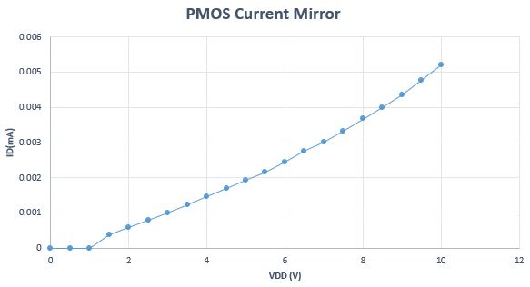
Image 7: Nmos (Left) and Pmos (Right) current measured with BMR circuit.


Image 8: Nmos (top) and Pmos (bottom) current simulation with BMR circuit.
From
the graphs it can be seen that the currents in both the nmos and pmos
are very close in the nA range, however they are slightly differnt from
each other. This still could just be an issue that the now three chips
interacting with each other have slight differences in them changing
what we expect to see.
After
measuring the current through each the nmos and pmos they were given a
load of two gate drain connected pmos/nmos and the current was measure
again.


Image 9: Nmos (Left) and Pmos (Right) current mirrors with two gate drain Pmos/Nmos load.
After getting the values they were made into excel plots and simulated in LTSpice as shown below.

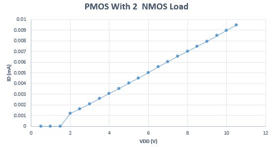
Image 10: Nmos (Left) and Pmos (Right) current measured with two gate drain Pmos/Nmos load.


Image 11: Nmos (top) and Pmos (bottom) current simulation with two gate drain Pmos/Nmos load.
This
experiment is the farest off from the simulation and the final values
are off by large factors. This could be due to the chip variations with
the now three chips being used to create this experiment. Additionally
the resistor could have been the wrong value but with no load the issue
wasnt as apparent as it is with the two pmos and nmos loads.
Return to EE 420L Home
Return to EE 420L Student Reports