
Lab 8 - EE 420L
Lab Report
Part 1
For the first part of characterizing the nmos the VDS was set at 3 and VGS was incremented in .1V steps from 0V to 3V in the following circuit
Image 1: NMOS circuit testing ID v. VGS
To measure current in the circuit an ammeter was connect so that the positive feed was at the source of the nmos and the negative lead went to ground. From the experimental conditions mentioned above the following excel graph was compiled.

Image 2: NMOS ID v VGS excel points ploted.
For comparison here is the LTSpice simulation from the level 1 model made in part 3.

Image 3: NMOS ID v VGS LTSpice simulation.
Next the NMOS was tested with VGS varying from 1V to 5V with VDS varying from 0V to 5V in .1V increments again in the following circuit.
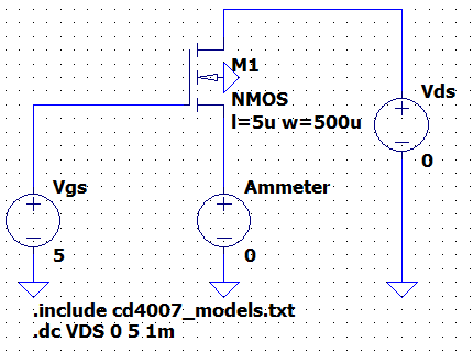
Image 4: ID v. VDS (0 < VDS < 5 V) for VGS varying from 1 to 5 V in 1 V steps circuit.
The experimented values were put into excel and the following graphs were generated. For reference all of the LTSpice simulations using the model made in part 3 will be shown after all of the excel graphs.

Image 5: ID v. VDS, VGS = 1, with VDS varying in .1V increments.

Image 6: ID v. VDS, VGS = 2, with VDS varying in .1V increments.

Image 7: ID v. VDS, VGS = 3, with VDS varying in .1V increments.

Image 8: ID v. VDS, VGS = 4, with VDS varying in .1V increments.

Image 9: ID v. VDS, VGS = 5, with VDS varying in .1V increments.

Image 10: ID v VDS LTSpice simulations.
From the experimental values it can be seen that as VDS increase the amount of current for the same VGS significantly increase.
The next step was to test ID v. VGS (0 < VGS < 5 V) with VDS = 5 V for VSB varying from 0 to 3 V in 1 V steps in the following circuit.

Image 11: ID v. VGS circuit.
After getting the experimental values they were plugged into excel and the following images were generated. Additionally all of the grpahs were resimulated using the LTSpice model made in part 3 and are shown in referenec after all of the excel graphs.

Image 12: ID v. VGS, VDS = 0, with VGS varying in .1V increments.

Image 13: ID v. VGS, VDS = 1, with VGS varying in .1V increments.

Image 14: ID v. VGS, VDS = 2, with VGS varying in .1V increments.
Image 15: ID v. VGS, VDS = 3, with VGS varying in .1V increments.

Image 16: ID v VGS LTSpice simulation.
From the above experiments it can be concluded that as VDS increases the threshold voltage increases.
____________________________________________________________________________________________________________
Part 2
The second portion of the lab will replicated everythign done to the NMOS but instead using the PMOS on the chip.
For the first step of the PMOS characterization we will test ID v. VGS (0 < VGS < 3 V) with VDS = 3 V in the following circuit.

Image 17: PMOS, ID v. VGS (0 < VGS < 3 V) with VDS = 3 V circuit.
After for getting the experimental values the following excel graph was made.

Image 18: ID v. VGS (0 < VGS < 3 V) with VDS = 3 V excel graph.
After the model was created in part 3 the circuit was resimulated for reference with the excel graphs.

Image 19: ID v VGS LTSpice simulation
The next step of the lab was to experimentally test ID v. VDS (0 < VDS < 5 V) for VGS varying from 1 to 5 V in 1 V steps in the following circuit.

Image 20: ID v. VDS (0 < VDS < 5 V) for VGS varying from 1 to 5 V in 1 V steps circuit.
After obtaining the values experimentally the following excel graphs were created.

Image 21: ID v. VDS (0 < VDS < 5 V) for VGS = 1

Image 22: ID v. VDS (0 < VDS < 5 V) for VGS = 2

Image 23: ID v. VDS (0 < VDS < 5 V) for VGS = 3

Image 24: ID v. VDS (0 < VDS < 5 V) for VGS = 4

Image 25: ID v. VDS (0 < VDS < 5 V) for VGS = 5
After the model was created in part 3 the circuit was resimulated for reference with the excel graphs.

Image 26: ID v VDS LTSpice simulation
Like the NMOS it can be seen that as VGS increases the circuit measured from the same voltage of VDS increases.
For the final characterization of the PMOS we tested ID v. VGS (0 < VGS < 5 V) with VDS = 5 V for VSB varying from 0 to 3 V in 1 V steps in the following circuit.

Image 27: ID v. VGS (0 < VGS < 5 V) with VDS = 5 V for VSB varying from 0 to 3 V in 1 V steps circuit.
The experimental values for this last step in the pmos were not obtained as the experimental values were not even close to anything that was expected.
______________________________________________________________________________________________________
Part 3
The first step of part 3 was to create an inverter using both the nmos and pmos and to measure the time delay with the following circuit.

Image 28: Inverter Schematic.

Image 29: Inverter time delay measured.
Additionally after the spice model was created the ciruit was resimulated and the following graph was made.

Image 30: Inverter LTSpice simulation
To make the level 1 spice model the following characteristics are needed: Tox, Vto, Kp, Gamma, and Lambda which can be obtained from the experiments above. To calculate Tox it is assumed w/l = 100 and Cox = 5pF, and all of the above values can be seen calculated below.


Image 29: LTspice text Level 1 Spice Model