EE 420L
Engineering Electronics II Lab
Lab
Project - Design of a Voltage Amplifier with a Gain of 10
email: matacarl@unlv.nevada.edu
5/08/19
Project description:
Design a voltage amplifier with
a gain of 10 using either the ZVN3306A or ZVP3306A (or both) MOSFETs and as many resistors and
capacitors as you need.
Project requirement:
·
Design a circuit using
a fast signal and driving a 1k load
·
Input resistance needs
to be greater than 50kΩ
·
Output swing as
large as possible
·
Design can pass a
100Hz input signal
·
Design should not
draw no more than 1mA under quiescent conditions from +9V power supply
The circuit design chosen is shown
below, the output of the common-source amplifier cascade into a common-drain
amplifier (source follower).
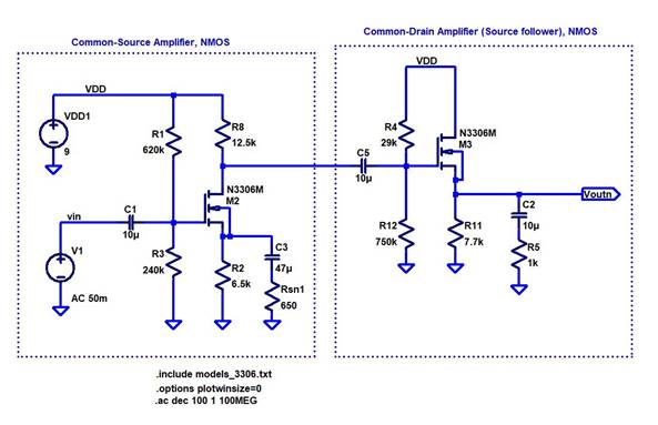
The reason for this design was to
maintain simplicity while still trying to meet all the requirements. But as we
will see later, there are several constrains with this design, especially on
the output swing.
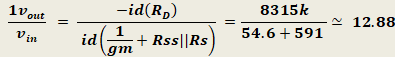
Hand calculations for common-source NMOS
For first stage we have
![]()
![]()
![]()
![]()
![]()
![]()
![]()
Gain
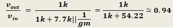
For Second stage
![]()
![]()
|
LtSpice simulaitons |
Experimental Results |
|
|
|
|
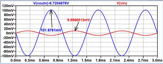
The simulation below shows the output having a gain of 10 (100mV),
when the input is 10mV.
|
|
|
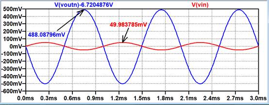
The simulation below shows the output having a gain of 10 (500mV),
when the input is 50mV
|
|
|
The simulation below shows the output starting to rail when the
input is 100mV.
|
|
|
The simulation below shows the max output swing.
|
|
|
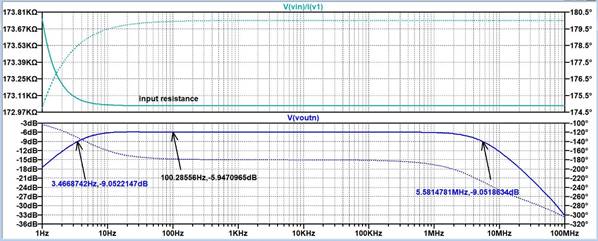
The bottom plot below shows the frequency response passing 100Hz with
a bandwidth over 5.5MHz, and the top plot shows the input resistance over 50kΩ
|
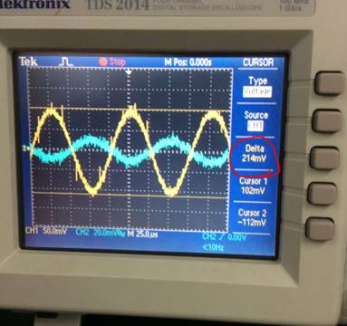
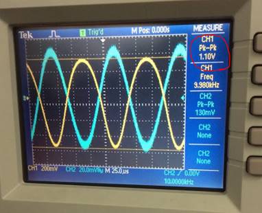
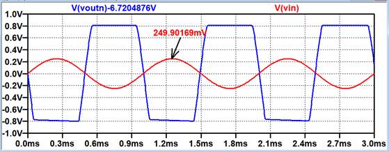
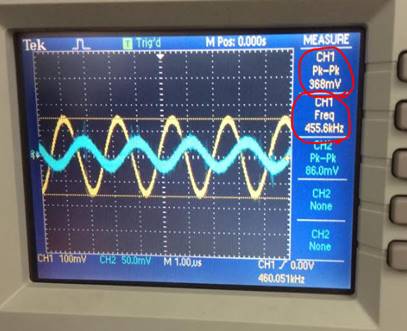
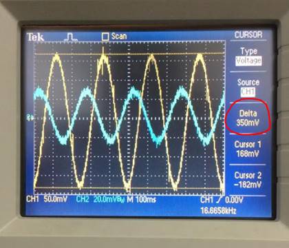
Below are two pictures showing
the upper and lower 3dB respectively. Input is 50mV and output should be
500mV, but at 3dB ≃353mV Upper 3dB
Lower 3dB
|
|
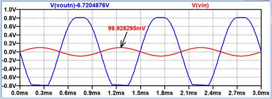
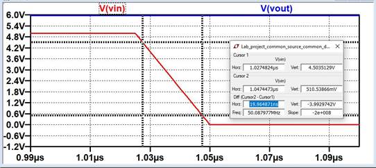
The plots below show the input fall time and output rise time. The
input signal is being simulated as the function generator fall time, and the
output is the risetime of the circuit being tested.
|
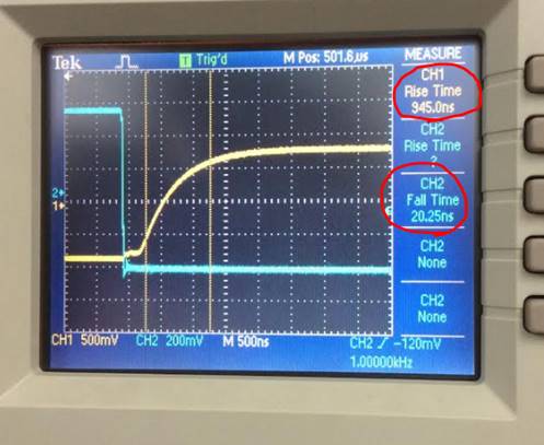
Below show the fall time of the function generator and the rise time
the circuit.
|
|
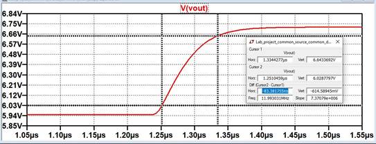
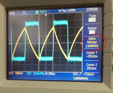
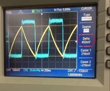
The plot below shows the slew rate to be around 0.864V/1𝞵s
|
|
|
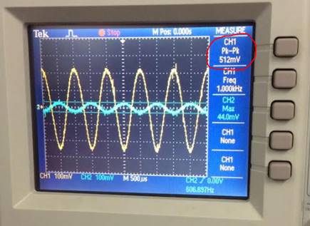
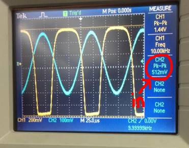
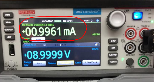
This design is barely meeting the quiescent requirement of 1mA. The
photo below shows this condition.
|
|
|
Comments: As we can see from the experiment results, this is not a good design
to follow if we want to meet the set requirements. The gain requirement can
be simple to accomplish with only one single common-source amplifier; however,
it pulls more than 1mA at quiescent conditions. Also, the output swing was poor,
because the first stage amplified but the second stage kill the gain. Which
in the beginning that was the plan because I wanted to move the drain and
source voltage up and down without changing the gain much. This did not work due
to the input resistance of the second stage affecting the output resistance
of the first stage. |
|
Return to student lab reports
Return to labs