EE 420L Engineering Electronics II Lab
Lab 3- Op–amps I, basic topologies, finite gain, and offset
email: matacarl@unlv.nevada.edu
2/20/19
Pre-lab:
- Watch
the video op_amps_I,
review op_amps_I.pdf (associated
notes), and simulate the circuits in op_amps_I.zip.
- Read
the write-up seen below before coming to lab.
Lab description:
This goal of this lab is to understand and test basic op-amp
topologies, find gains, and obtain offsets. The op-amp used for this lab is
LM324.
Part 1: Questions regarding LM324 datasheet
For
the following questions and experiments assume VCC+ = +5V and VCC- = 0V.
a)
Knowing the non-inverting input, Vp, is
at the same potential as the inverting input, Vm,
(called the common-mode voltage, VCM) what are the maximum and minimum
allowable common-mode voltages?
By
looking at the table below from the datasheet the maximum VCM is 5-1.5 = 3.5V,
and the minimum is zero; however, those values are only for ambient temperature
of +25 degrees Celsius.

b) What is a
good estimate for the op-amp's open-loop gain?
A good open-loop
gain at +25°C ambient temperature is 100V/mV
By
looking at the plot below from the datasheet we can see the open loop gain, and
we can see that at around 10Hz the output is at about 100dB, which is about a
gain of 100000 ![]() .
.

c) What is a
good estimate for the offset voltage? For worst case
design what value would you use?
A good estimated for good offset voltage is 2mV, but for worst case
design 9mV would be chosen; this is seen in the table below from the datasheet.

Part 2: Build, and test, the following circuit. Note
that a precise value for the 5k resistors isn't important. You can
use 4.7k or a 5.1k resistors

a)
What is the common-mode voltage, VCM? Does VCM change? Why or why
not?
The common-mode
voltage in this circuit is 2.5V, and this does not change because is a DC
voltage divider. However, if VCC changes the VCM will be half of that voltage,
that is VCC/2. Also, the decoupling capacitors are keeping the voltage at a
steadier state if there is noise in the line or spikes.
b) What is
the ideal closed-loop gain?
![]()
c) What
happens if the input isn't centered around VCM, that is, 2.5 V?
-
What is the output swing and what is it centered around?
-
Provide a detailed
discussion illustrating that you understand what is going on.
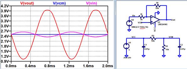
The
snapshot on the left shows the input (yellow) and output (blue) with AC
coupling. We can see that the output is inverted. The one on the right shows
both again, but this time with the DC offset of 2.5V. Both, input and output
are swinging around 2.5V. The gain we are using is 1, (5k/5k). If the input has
an amplitude of 100mV, then the output has an amplitude of 100mV as well, but
it’s inverted.


If the
output isn’t center around VCM then there’s a difference in voltage between
input offset and the inverting input of the op-amp, which will affect the
current, and ultimately the output offset swing.
The plot,
schematic, and snapshot show the result if VCM stays at 2.5V and Vin offset
changes to 4V. The output (blue) is now swinging at around 1V.


We can
use the KCL formula to demonstrate the reason for the output swinging at 1V DC.

The plot,
schematic, and snapshot show the result if VCM stays at 2.5V and Vin offset
changes to 2V. The output (blue) is now swinging at around 3V.


Again, we can use the KCL formula to
demonstrate the reason for the output swinging at around 3V DC.

d)
What is the maximum allowable input signal amplitude? Why?
From the
datasheet we know that the maximum offset we can add to the input is VCC-1.5 =
3.5V. So if we had a VCM of 3.5V, then the input swing
amplitude can only go up to 1.5V. Now if we apply that swing voltage to a VCM
of 2.5V then the output swing will start clipping at around 4V. Which is about
1.5V up from the VCM of 2.5V. This can be seen in the simulation below as well
as the photo from the oscilloscope


e)
What is the maximum
allowable input signal if the magnitude of the gain is increased to 10? Why?
If we had a gain of 10, and we know that
the maximum swing is 1.5V then the maximum input we can have is 150mV
![]()
We can see that if a signal of 150mV is
applied to the input then then output will be around 1.5V, which is the voltage
at which will start clipping.
The plot on the left shows the input with a
magnitude of 150mV, and the output starting to clip. The plot on the right
shows the input with a magnitude of 170mV,
which cause the output to clip because the
swing is about 1.7V (10*0.170).

f)
What is the point of the 0.01 uF
capacitors from VCC and VCM to ground?
-
Are these values critical or could 0.1 uF,
1,000 pF, 1 uF, etc. capacitors be used?
The point
of the capacitors here are to use them as decoupling capacitors to provide a
more constant voltage. In a way they act as constant battery source. Any spikes
on the power supply will be minimized by the capacitors. The only concern is at
initial condition when the power supply is switched on, which will have a RC
time.
Below we
have given an initial condition to VCM to see its RC time, when the power
supply has barely been turned on.

g)
The data sheet shows that this op-amp has an input bias current
that flows out of the op-amp's inputs of typically 20 nA.
-
This current flow out of both the non-inverting and inverting
inputs through the resistors connected to these inputs.
-
Show how the operation of the circuit can be affected if, for
example, R1 and R2, are much larger. Explain what is going on.
-
What is the input offset current? What does this term describe?
The input
bias current is DC current that will cause a voltage drop across the resistors
which will affect the output offset voltage. The higher the resistor the higher
the smaller the current that flows through R1 and R2. This decrement in current
as it gets closer to the input bias current will have an increase in the VCM
voltage. We are using 10MEG resistor to see the difference between the input
offset and the output offset.
As we can
see in the simulation below, Vout has a higher offset
voltage because replacing R1 and R2 with 10MEG resistors caused VCM to
increase.


The current flowing thorough R1 and R2 without
adding the input bias current would be close to 250nA
![]()
Current flowing through R1 after adding bias
current
![]()
![]()
Now if we apply KCL again we can see that the DC
offset of Vout increases

The photo
on the left shows the input and output with AC coupling to demonstrate that
changes don’t affect much the AC signal, but mostly the DC signal, which is
shown on the right. The picture on the right has been set up with DC coupling
to show that Vout (blue) has a higher DC offset
voltage than the input DC offset.


-
What is
the input offset current? What does this term describe?
The input offset current is the small DC current
difference between the inverting and noninverting inputs.
Part 3: Testing the Offset Voltage
Explain how the following
circuit can be used to measure the op-amp's offset voltage.
The typical offset voltage known from the datasheet is about 2mV
at +25 °C, and if we want to clearly see this voltage then we must increase the
gain. As we can see from the circuit, the input voltage for the inverting
topology has changed to the same as VCM. So, if there is an offset voltage,
then it will be increased by the gain and Vout will
be equal to the gain plus 2.5V.


Could
be modeled as this
or just as this
![]()
![]()
We can just apply KCL to find the difference
in DC offset between the output and the input.

Below is
the schematic and plot used to simulate the difference between offsets


Below is
a photo of the input and output using 100k and 1k for RF and RI respectively.

Since we
could barely see the difference, we decided to use 1MEG resistor as RF. However, doing this affected the current
flowing out of the inverting input of the op-amp, and gave us a DC offset lower
than the input DC offset. The 1MEG ohm
resistor was used to calculate the offset of 4 different op-amps.
LM324 op-amp, RI =1k, RF=1MEG UA 741
op-amp, RI =1k, RF=1MEG


LM 741 op-amp, RI =1k, RF=1MEG LM 348
op-amp, RI =1k, RF=1MEG


Offset voltage Experimental results
|
Op-amps |
Input |
Output |
Offset
difference |
|
LM324 |
2.62V |
1.36V |
1.26V |
|
UA 741 |
1.99V |
1.73V |
0.26V |
|
LM741 |
2.68V |
4.52V |
1.84V |
|
LM348 |
2.68V |
3.72V |
1.04 |
Return to student lab
reports
Return to labs