Project - ECE 420L
Authored
by Kyle Butler, butlerk2@unlv.nevada.edu
4/24/2019
Project – design a voltage amplifier with a gain of 10 using either the ZVN3306A or ZVP3306A (or both) MOSFETs and as many resistors and capacitors as you need.
You should try to get as fast a design as possible driving a 1k load,
with an input resistance greater than 50k, with as large of output
swing as possible.
AC coupling input and output is okay as long as your
design can pass a 100 Hz input signal. Your report, in html, should
detail your design considerations, and measured results showing the amplifier's performance.
Your
design can draw no more, under quiescent conditions (no input signal),
than 1 mA from a +9 V supply voltage. Your report is due at the beginning of lab on Wednesday, May 8. Access to your CMOSedu.com lab accounts will be removed at this time.
------------------------------------------------------------------------------------------------------------------------------------------------------------------------------------------------------------------
To
begin this design I review previous labs, specifically lab 6, in order
to help make a decision as to which topology would be the best base for
this project.
A push-pull amplifiier can be used as a transimpedance amplifier because it has a high gain and can drive a load.
The
limiting parameter in this design is a draw of less than 1 mA from a
+9V power supply, for this design we will use 0.8mA. Additionaly we
need to ensure an input resistance greater than 50k, which will not be
an issue for a push-pull topology because the input resistance is so
great.
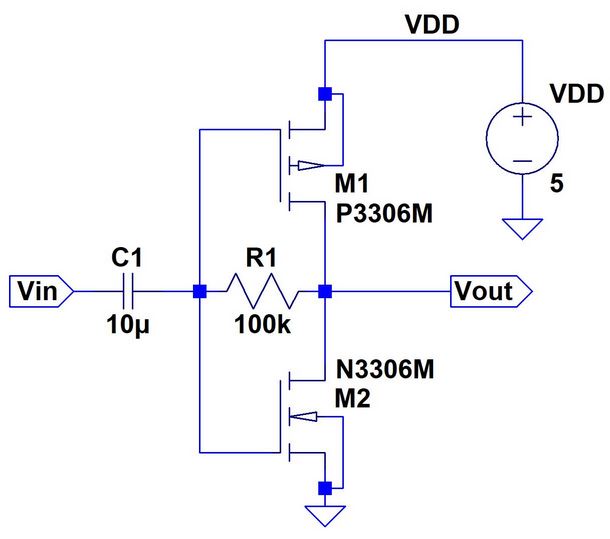
Push-Pull design from Lab 6:
From
this design we can see there is no limiting resistor from VDD to ground
except transconductance(gm). Which is a small resistance and will
result in a large current draw.
In order to control the current
draw a current limiting resistor will be added to the source of the
NMOS, however since this resistance will be used in the gain
calculation it may be neccessary to split the resistor with the source
of the PMOS in order to help share the limitinng of the current draw.
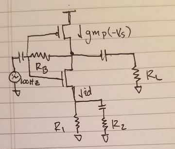
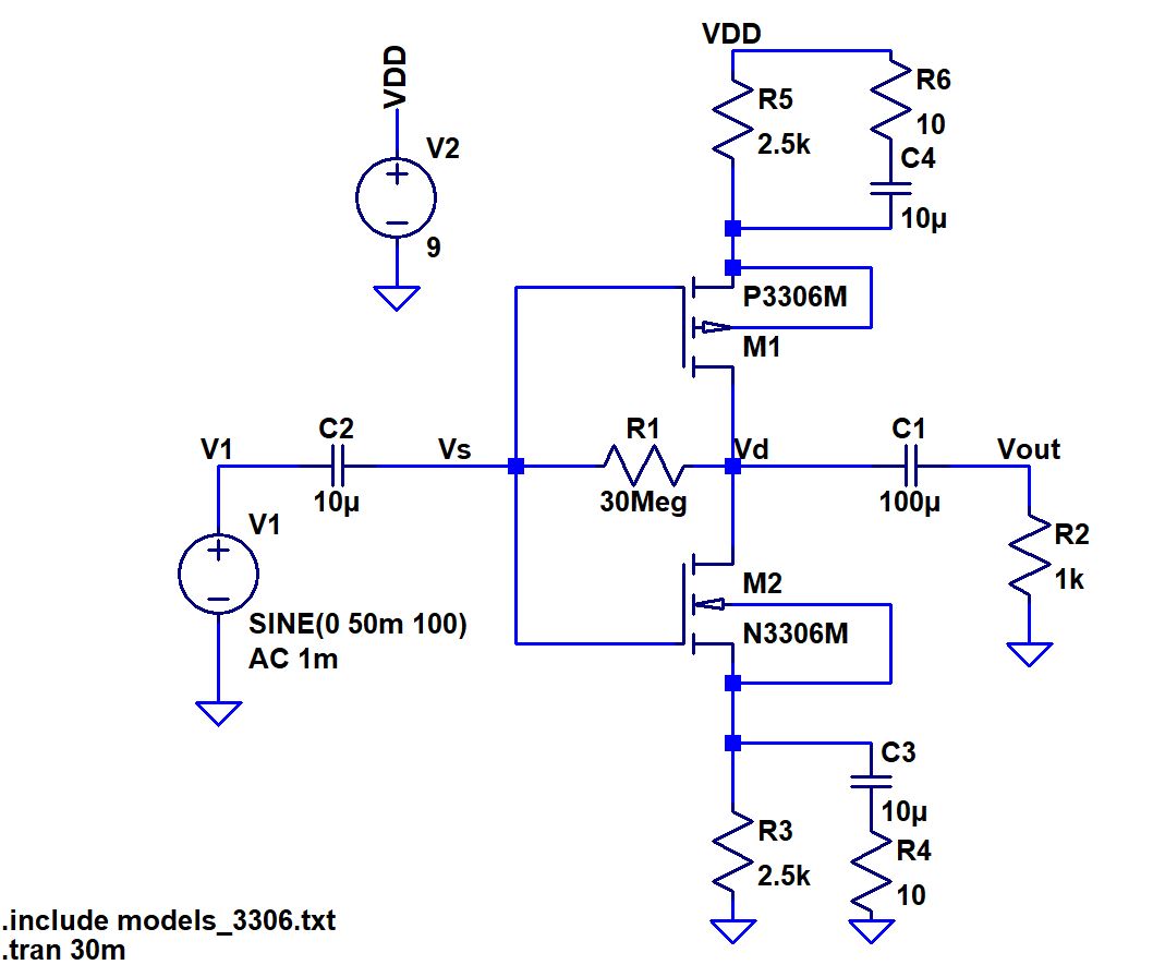
General Schematic for Design
The
resistor RB has no effect on the gain or current draw, just the input
resistor. This means the larger resistor we chose the larger the input
resistance we will recieve. Because of the lab supplies we chose a
30MEG resistor for Rb.
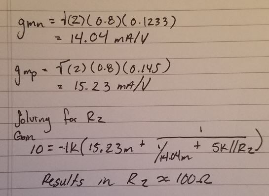
Before we begin hand calculations to find good values for R1 and R2 we need to know some parameters of these transistors.
From spice models in lab 6:
| Kpn = 0.1233 | Vthn = 1.824V |
| Kpp = 0.145 | Vthp = 2.875V |
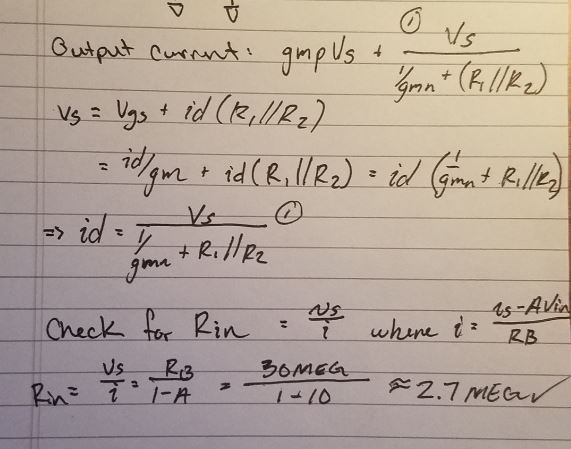
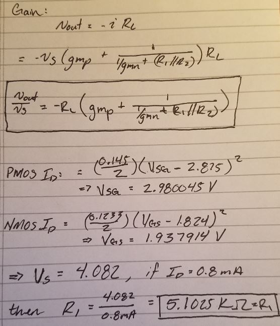
Now lets find an expression for drain current as well as gain.
Hand Calculations:
From the hand calculations above we should select R1=5K Ohms, R2=100 Ohms, and RB = 30MEG.
Lets
test these values in the simulations, remeber we need to split the 5K
and 100 Ohms resistors on the source of both the PMOS and NMOS.
Simulation:
Notice
the capacitors are addec to seperate the resistors in DC and allow for
fine adjustments in AC, similar to placeing a potentiometer in line.
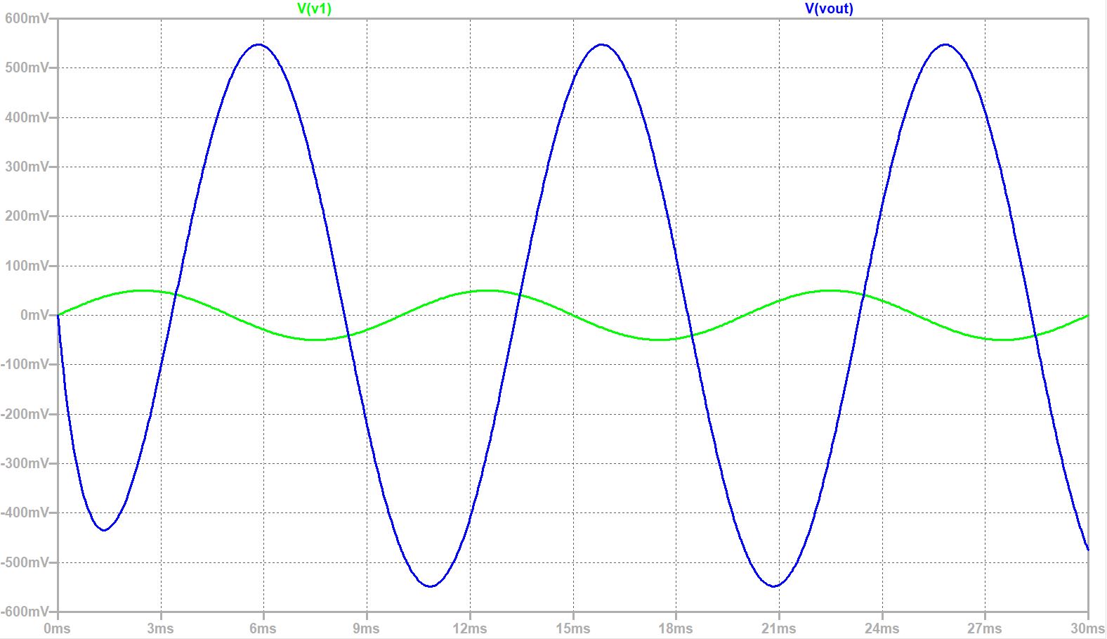
Results:
Here
we are able to see a gain of approximately 11. This is fine because we
are expecting a drop between simulation and gain and experimental gain
from past experiements. Increasing R4 and R6 to 55ohms will result in a
gain of 10.
It may be neccsarry to reduce R3 and R5 in order to be able to vary the gain since R4/R6 are already at such a low value.
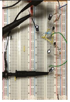
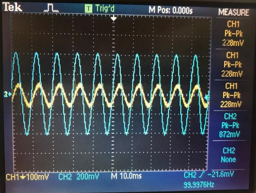
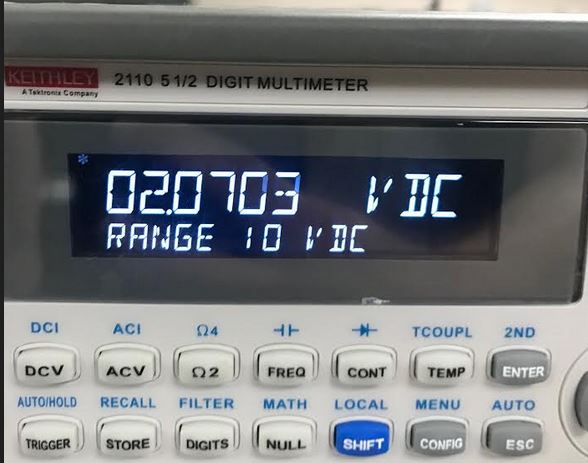
Experimental:
Circuit
Gain
Current = Vdrop/Resistor
From
the images above we can see an approximate gain of 8.7. The input
signal on the image reads 228mV, but it is acutally 100mV and there is
some error on the oscilloscopes automatic measuring. Additionaly we had
to use 2.2K resistors for R3/R5 because there were no 2.5K resistors in
the lab at the time.
This results in a current of 2.07/2200 = 0.94mA. This meets the threshold for the current limitation.
We
very nearly met all of the requirements for this lab, unfortunatley we
are a little short on the gain. I beleive this is due to the 20% error
allowed in these resistors and must have changed the over all
experimental gain. This push-pull topology is very sensitive when
refering to the allow flucuation on the resistor value.
This lab
demonstrated how the push-pull amplifier can draw very littler current
because of its large input resistance and effectiverly amplifiy a
signal. In fact I have recently used this design to amplify the output
of a microcontroller specificaly because the low current draw will not
over draw current from the board.
Return to butlerk2 EE 420L Reports
Return to EE 420L Labs