Lab 9 - ECE 420L
Authored
by Kyle Butler, butlerk2@unlv.nevada.edu
4/24/2019
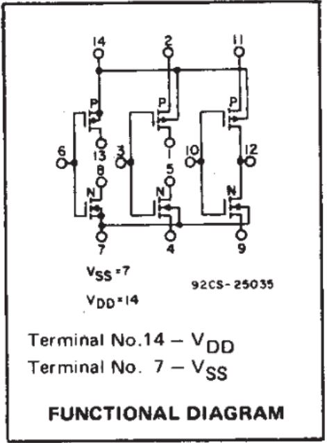
Design of a Beta-Multiplier Reference (BMR) using the CD4007UB CMOS transistor array
Pre-lab Work
- This lab will use the level =1 MOSFET model created in lab 8 and, again, the MOSFETs in the CD4007UB transistor array.
- Design and simulate the operation of a BMR that biases the NMOS devices tso that they have a gm of 20uA/V.
- Use a simple (big) resistor to VDD for the start-up circuit (explain how the addition of a resistor ensures start-up).
- When
the BMR is operating the current in the big resistor should be muich
smaller than the current flowing in each branch of the BMR
- Write-up, similar to a homework assignment, your design calculations and simulation results.(This will count as the pre-lab quiz.)
- Ensure that you show the following in what you turn in:
- Hand calculations
- Operation as VDD is swept from 0 to 10V
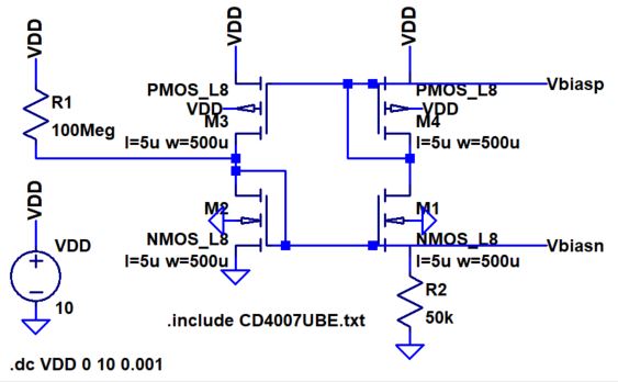
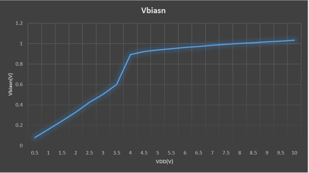
- Vbaiusn
should stabilize (be constant) after VDD hits a minimum value (estimate
this value of VDD assuming VGS/VSG is a threshold voltage and
VDS,sat/VSD,sat is zero).
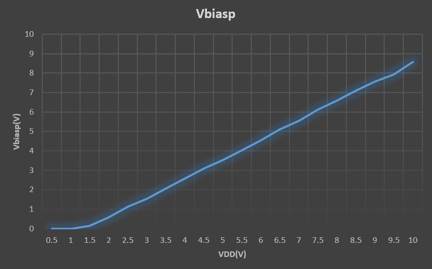
- Vbiasp should follow VDD after VDD hits a minimum value (show this in simulations)
- Unstable operation if too much capacitance is shunting the BMR's resistor (see bottom of page 630)
- Comments comparing the hand calculations with the simulation results
Lab Work
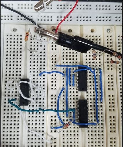
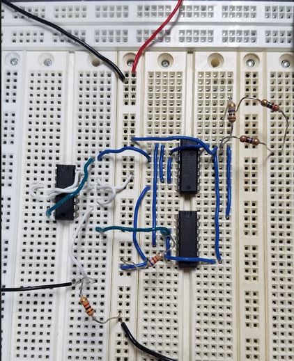
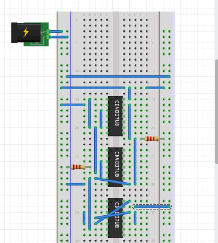
- Build your BMR
design and characterize it as you did in the pre-lab (if you use two chips ensure that grounds and VDDs of both chips are tied together).
- You
expect the BMR to become unstable if there is a large capacitance
across the resistor, such as a scope probe (important), so care must be
exercised
- Use your BMR to
bias, and thus create, a:
- NMOS
current mirror
- PMOS
current mirror
- Measure how the
current varies through each current mirror as the voltage across the
mirror changes.
- Of
course the current in the NMOS (PMOS) current mirror goes to zero as the
voltage on the drain of the output device moves towards ground (VDD)
- Using these current mirrors drive two gate-drain connected transistors
- For the first experiment use the NMOS current mirror to drive two PMOS gate-drain connected devices.
- Use
the voltages on the gate-drain connection of the two devices to bias a
cascode current mirror (characterize this mirror as before)
- For the second experiment switch, that is, use the PMOS current mirror to drive two NMOS gate-drain connected devices.
- Again, use these two voltages to bias an NMOS cascode current mirror then characterize.
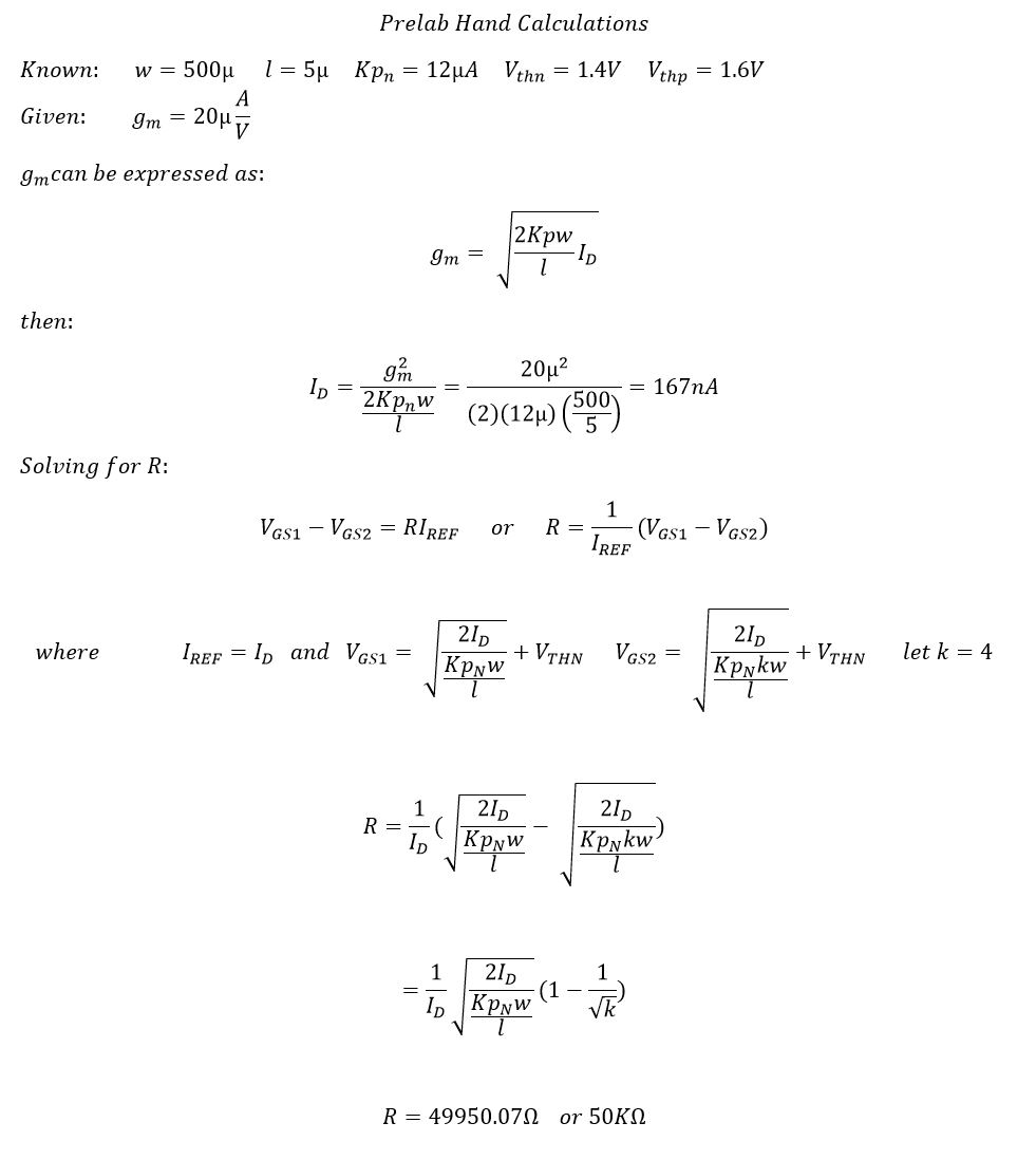
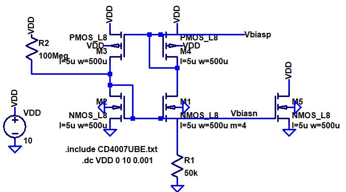
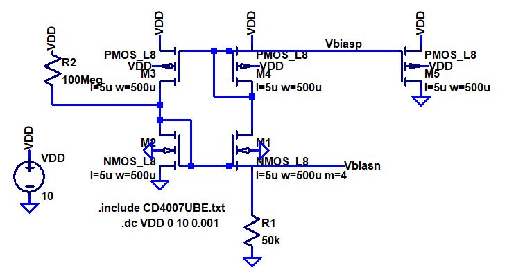
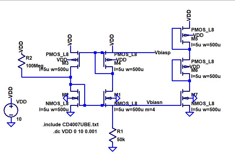
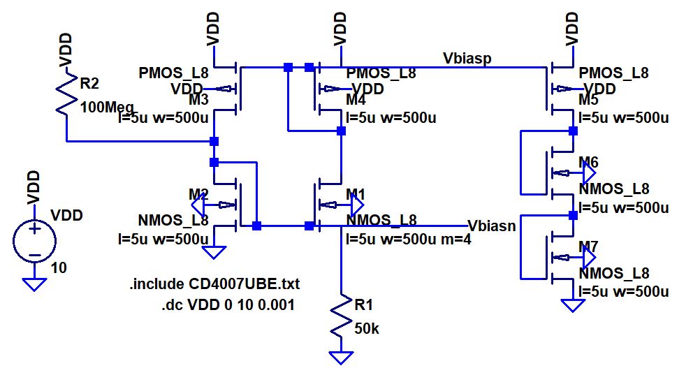
BMR Design
Schematic and Simulations:
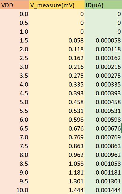
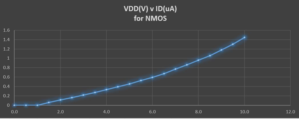
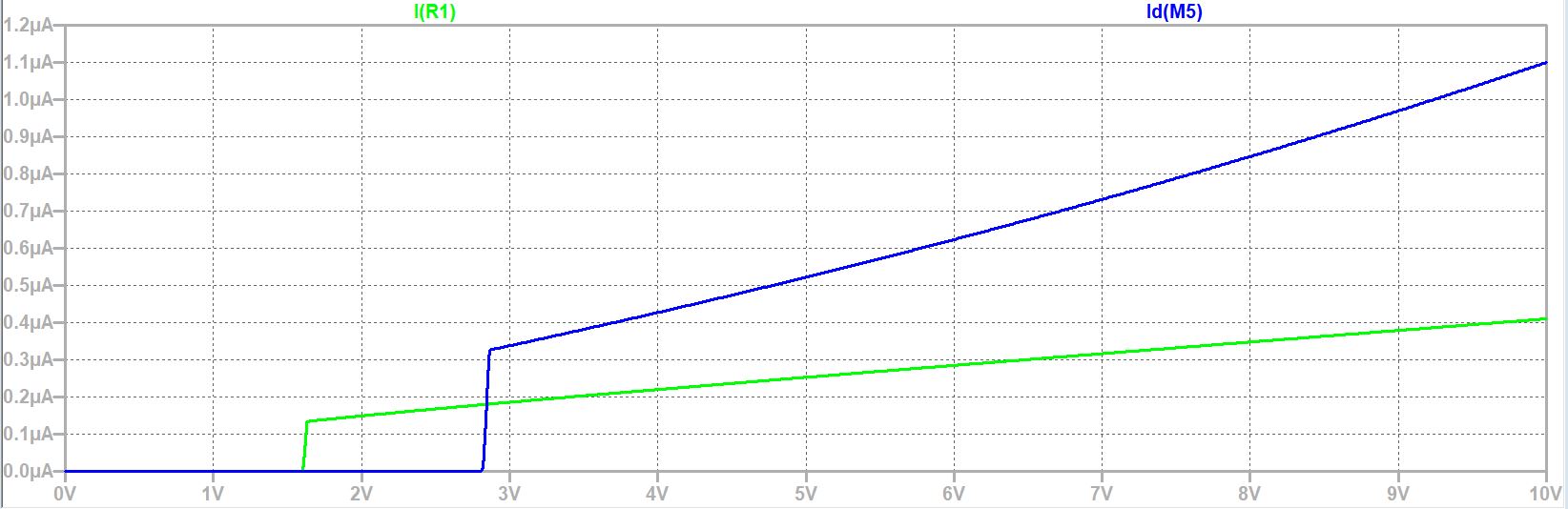
The
above simulations show the charateristics of the MOSFETs models. For
example, the threshold voltage is approx 1.4V and the drain current is
167nA at 10V.
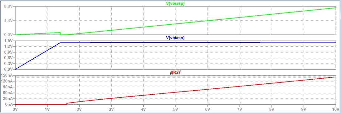
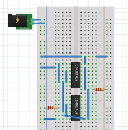
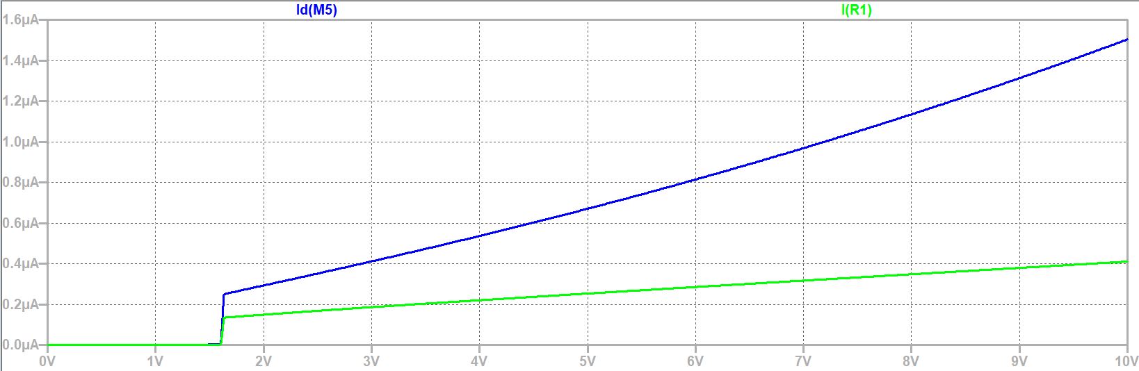
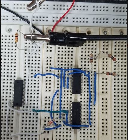
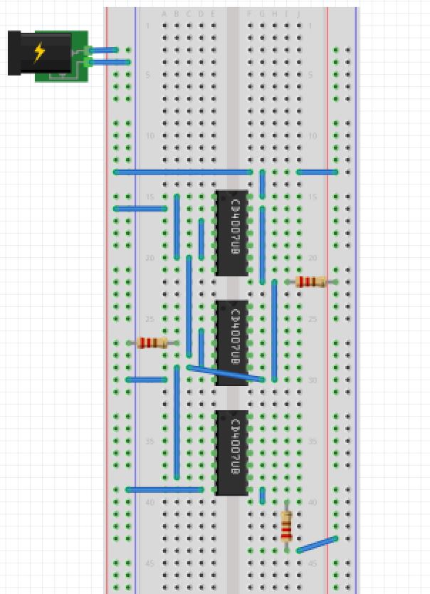
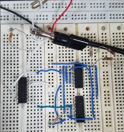
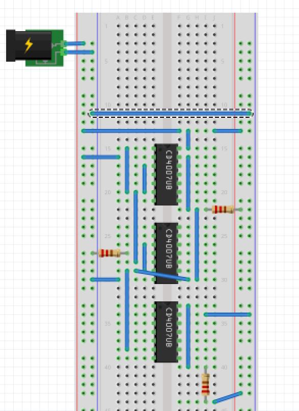
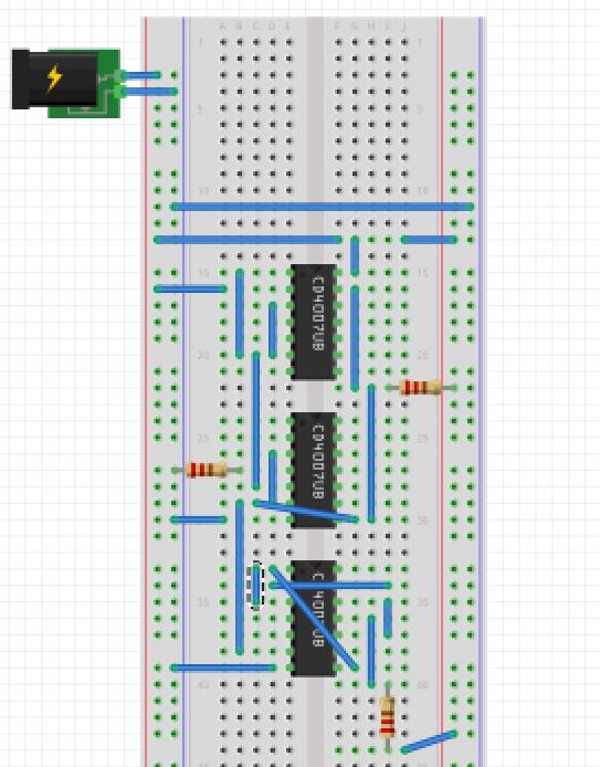
Experimental BMR
Schematic:
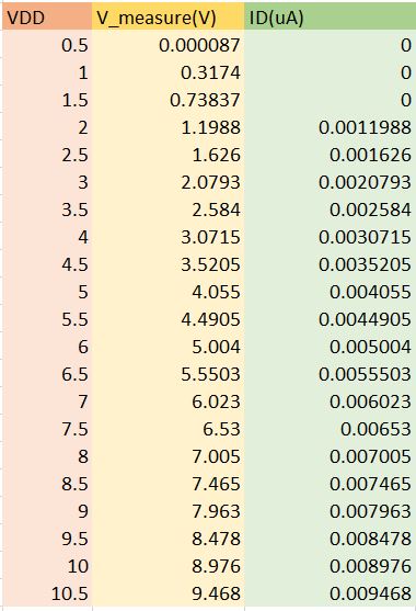
The
resistors on the right side of the CD4007UB chip represent the 100MEG
resistor in the simulation while the left side resistor is the 50k.
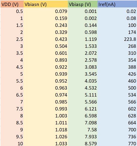
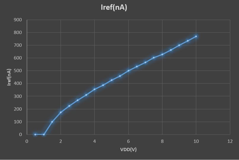
In
order to take these measurements we measure the voltage drop across the
50k resistor and divided that value by 50k for the Iref value, while we
simply probe the Vbiasn/p to ground with a multimeter to recored
Vbiasn/p.
A scope probe and oscilloscope could not be used because the BMR would become unstable.
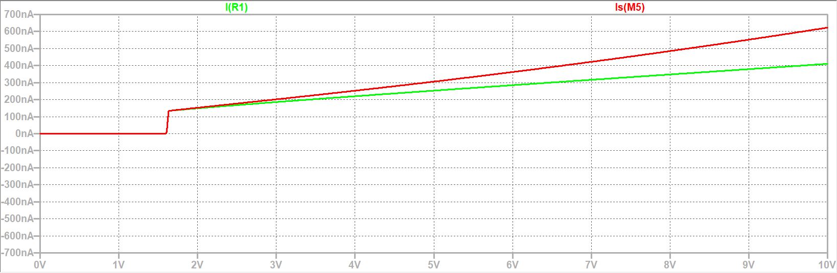
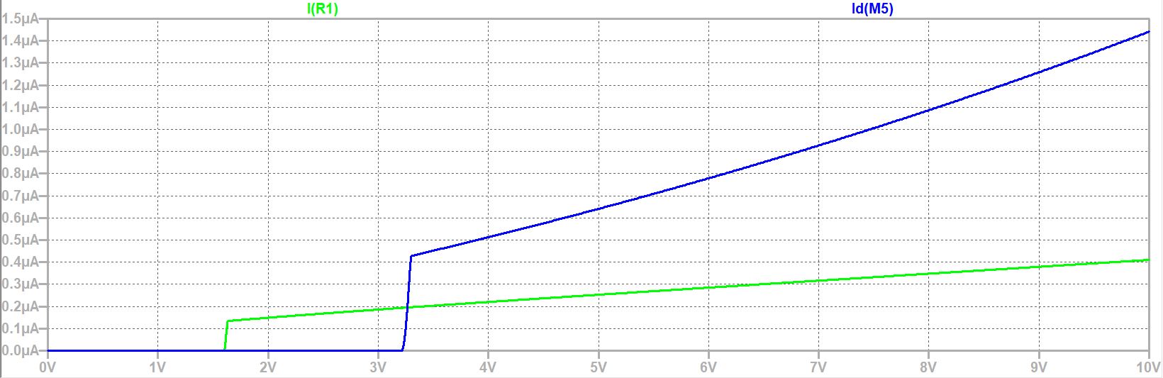
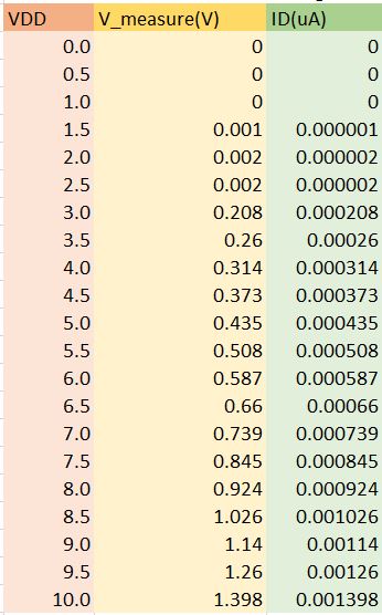
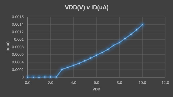
Results:
The
experimental current is slightly higher then the simulated values,
I beleive this is due to the resistor value being less then 50kOhms. If
the values of the resistor were correct, then we would need to reduce
the Kp values in the model simulations to compensate. Only Kp can be
changed to cause a change in Iref because the other values in the
equation of R are based on physical sizes of the MOSFETs. This can be
seen in the hand calculations above.
Current Mirrors
Nmos Current Mirror
Simulation:
Experimental:
In
order to measure the current through the mirror, a 1k resistor was
placed between the drain and VDD of the added NMOS. This measured
voltage was divided by the 1k resistance, resulting in current through
the mirror. This method was used because the ammeters in the lab were
uncappable of measureing current below a mA range.
Results:
The
simulated and experimental current are fairly close. This means our
characterization of the UD4007UB nmos is a good representation of the
actual chip.
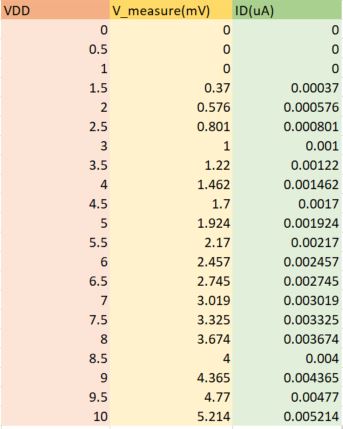
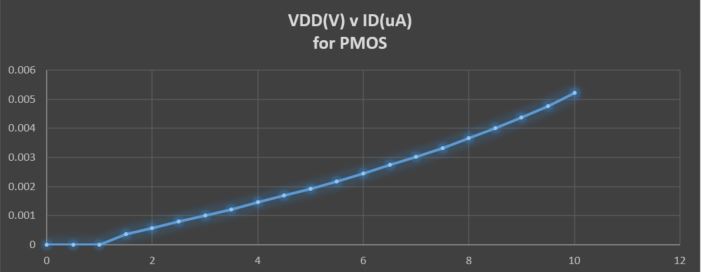
PMOS Current Mirror
Simulation:
Experimental:
The current through the pmos mirror was measured similarly to the nmirror above.
Results:
The
experimental and simulated ID differ by approx. 100nA at 10V. The
experimental results are higher than the simulated because the Kpp
characterized in Lab 8 needs to be reduced.
Current Mirrors Driving Two Gate-Drain Connected Transistors:
Nmos Current Mirror Driving 2 Pmos:
Simulations:
Experimental:
Results:
There
are some errors in this plot. The ID is actually plotted as mA instead
of uA, this will be changed in the future. Besides the incorrect labels
we can see that the ID of the experimental and simulated for the nmos
are again fairly close. They differ by approximately 0.05uA
Pmos Current Mirror Driving 2 Nmos:
Simulations:
Experimental:
Results:
This
is the greatest diviation between simulate and experimental current. ID
differs by approx. 0.15uA. The experimental plot should be labeled as
mA for ID instead of uA. This results in a 0.95uA for experimental and
1.1uA for simulated current.
Conclusion:
Some simulations and experimentaion results were not exact. We tried to
ensure that all the chips were from the same production lot, but the
markings on the chip did not indicate the date of the production lot.
This could be why our experimental results are different from our
simulation results.
The BMR was the closest interms of comparison, so it must be
the third chip added to the circuit that is causing the problem. I
believe closer results can by achieved with the same execution if the 3
CD4007UB chips were bought from the same production lot.
Another
possible error could be the parameters characterized in Lab,
specifically the value chosen for Kpp. The value for Kpn seems to be
correct when comparing the experimental and simulated results, but more
errors can be see when looking at Kpp.
Return to butlerk2 EE 420L Reports
Return to EE 420L Labs