Lab 7 - ECE 420L
Authored
by Kyle Butler, butlerk2@unlv.nevada.edu
4/3/2019
Pre-lab work:
- Review
the datasheet
for the CD4007.pdf
CMOS transistor array. (Not for this lab we used the CD4007UB because the lab did not have the CD4007)
- Ensure
that you understand how the bodies of the NMOS are tied to pin 7 (VSS,
generally the lowest potential in the circuit, say ground) and that the
bodies of the PMOS are tied to pin 14 (VDD, generally the highest
potential in the circuit, say + 5V).
Lab work:
In this lab you
will characterize the transistors in the CD4007UB and generate SPICE
Level=1 models. Assume that the MOSFETs will be used in the design of
circuits
powered by a single +5 V power supply. In other words, don't
characterize the devices at higher than +5 V voltages or lower than
ground potential.
- Experimentally
generate, for the NMOS device, plots of:
- ID v. VGS (0 < VGS < 3 V) with VDS = 3
V
- ID v. VDS (0 < VDS < 5 V) for VGS varying
from 1 to 5 V in 1 V steps, and
- ID v. VGS (0 < VGS < 5 V) with VDS = 5 V
for
VSB varying from 0 to 3 V in 1 V steps.
- Note
that for this last one, if VSS (NMOS body) is ground (again,
the
Body,
VB, is grounded) then the source voltage will be varied from 0 to 3 V
in 1 V steps to realize VSB ( = VS - VB = VS) varying from 0 to 3 V in
1 V steps. At the same time VGS will be varied from 0 to 3 V (when VS =
0), 1 to 4 V (when VS = 1 V), 2 to 5 V (when VS = 2 V), and 3
to 5
V (when VS = 3 V). In other words, as VS is increased by 1 V the VGS
has to shift up by 1 V as well
- Assuming
that the length of the NMOS is 5 um and its width is 500
um calculate the oxide thickness if Cox (= C'ox*W*L) = 5 pF.
- From
this measured data create a Level = 1 MOSFET model with (only)
parameters: VTO, GAMMA, KP, LAMBDA, and TOX.
- Compare
the experimentally measured data above (the 3 plots) to
LTspice-generated data (again, 3 plots) and adjust your model
accordingly to get better matching.
- Experimentally,
similar to what is seen on the datasheet (AC test circuits seen on page
3 of the datasheet), measure the delay of an inverter using these
devices (remember the loading of the scope probe is around 15 pF and
there is other stray capacitance, say another 10 pF).
- Using
your model simulate the delay of the inverter and compare to measured
results. Adjust your SPICE model to get better matching between the
experimental data and the measured data.
- Repeat
the above steps for the PMOS device where VDS, VGS, and VSB are
replaced with VSD, VSG, and VBS respectively.
Chip Pins Layout:
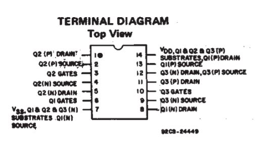
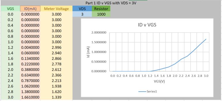
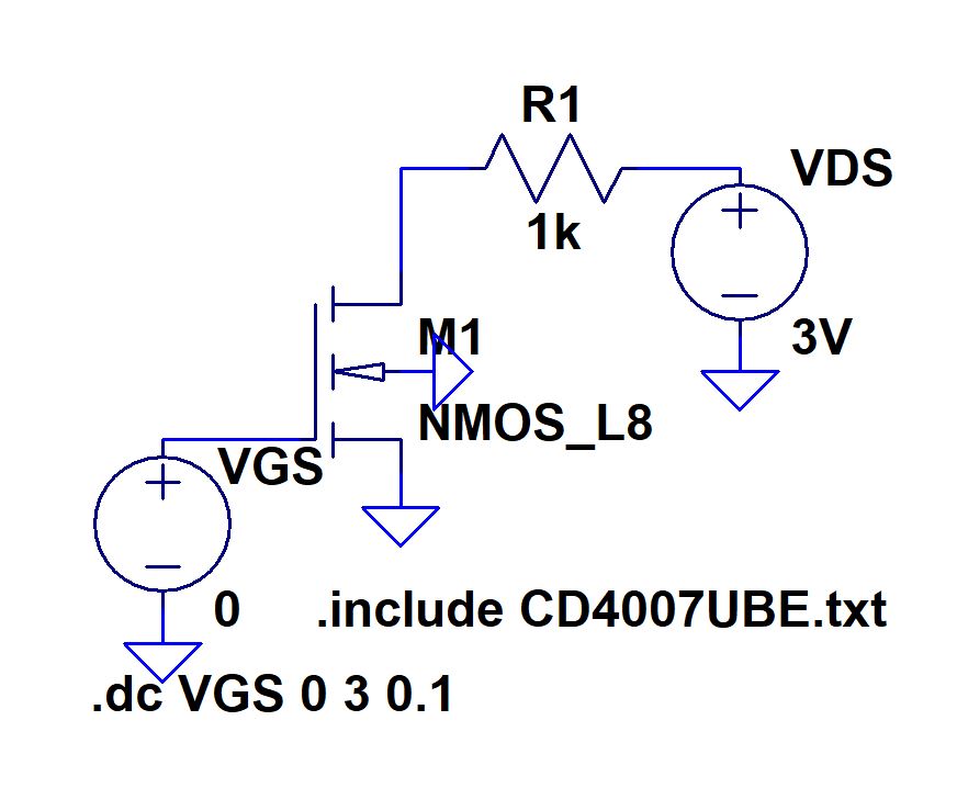
Part 1: NMOS device plots:
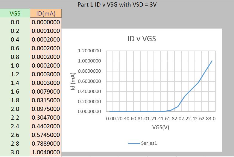
1. ID v. VGS (0<VGS<3V) with VDS = 3V
In
order to generate this plot the drain (pin 5) will see 3V. Between the
3V and pin5 we placed a 1k resistor to measure the voltage drop and
therefor the current through the drain (ID). The source (pin 4) was
grounded and the gate (pin 3) sees 0V initially and is incremented in
0.2V steps to 5V
Below the data points and excel graph can be seen:
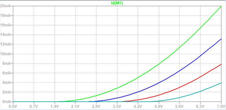
This is the expected shape of the response curve when plotting ID v. VGS. Note the ID is scaled to mA instead of uA.
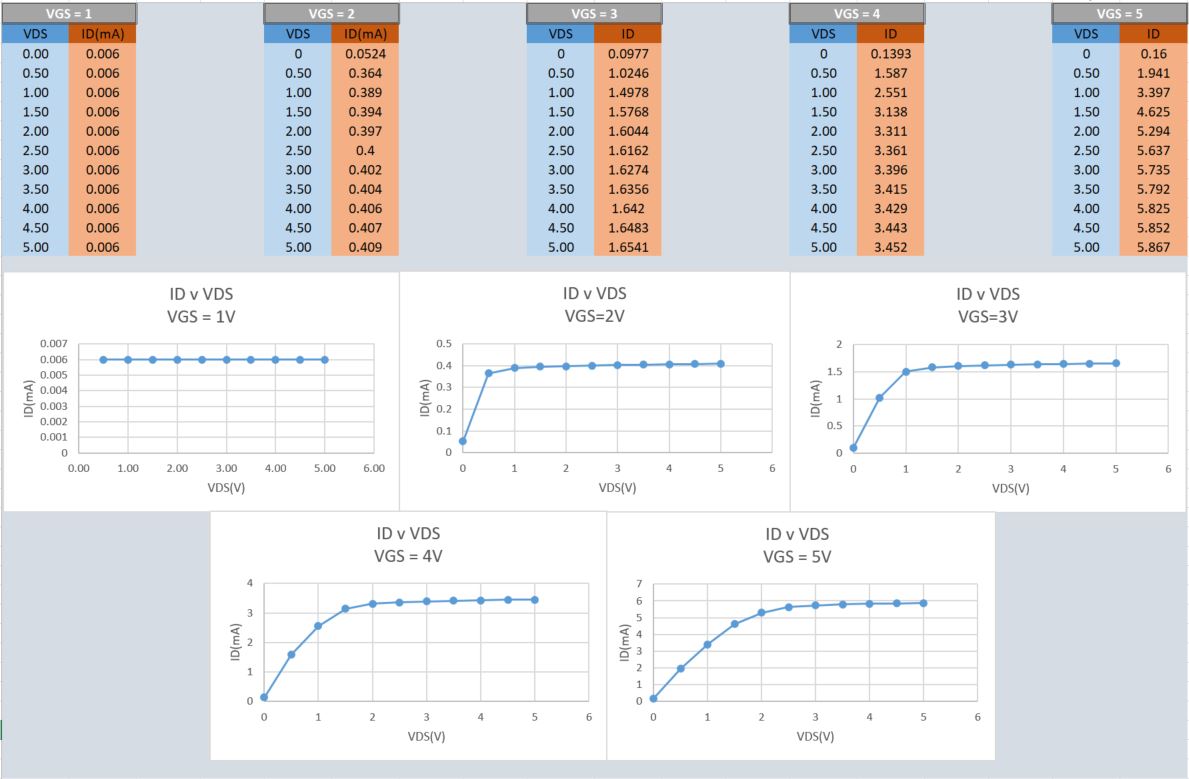
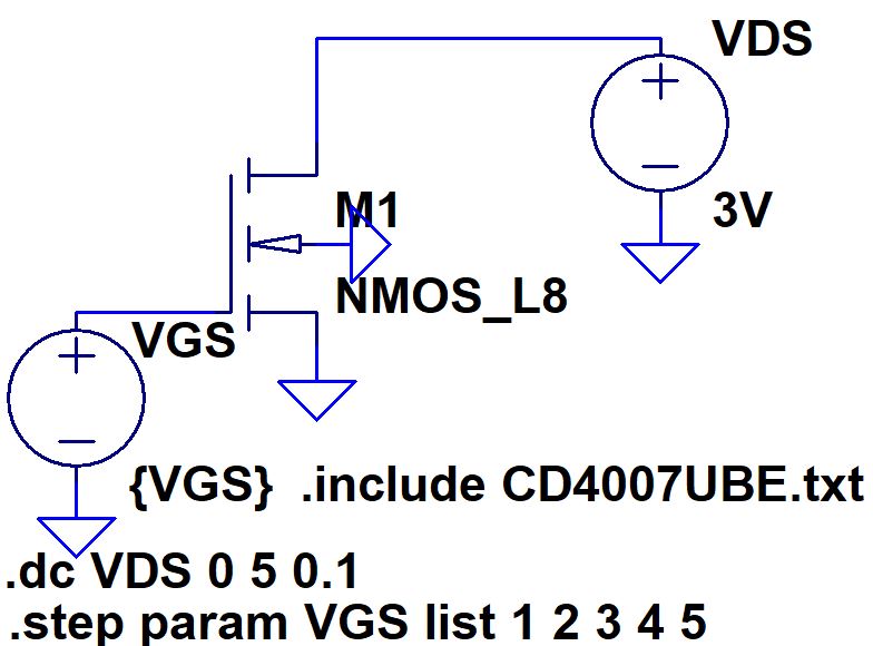
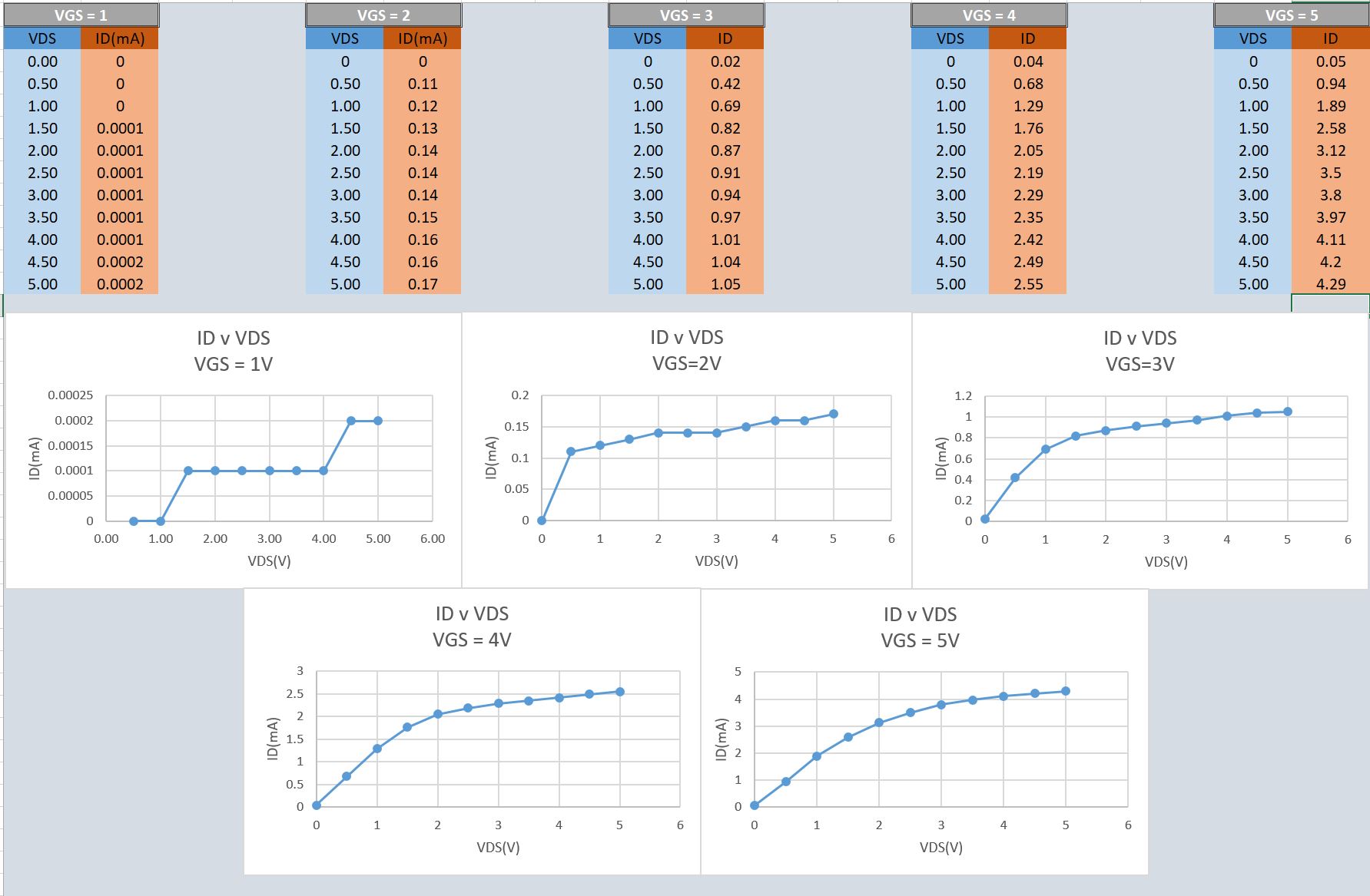
2. ID v. VDS(0<VDS<5V) with VGS varying from 1 to 5V in 1V steps.
In
order to generate this plot the drain (pin 5) will see 0-5V. While the
gate (pin 3) will see 1-5V in 1V steps and the source (pin4) is
grounded.
Additionally we decided to simply probe the drain to
measure ID. This is done by completeing the connection between the
sweeping power supply and pin 5, such that the current passes through
the Ammeter
Below the data points and excel graph can be seen:
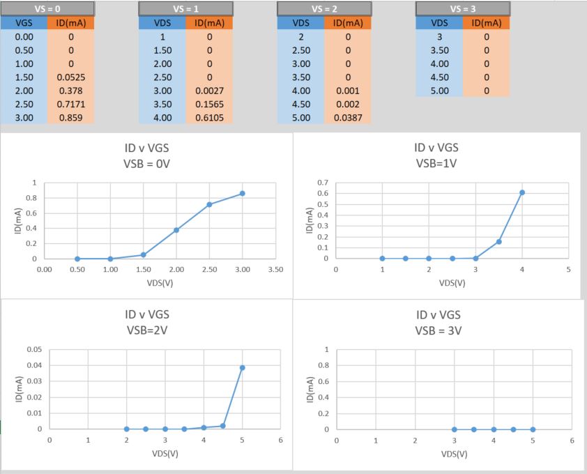
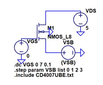
3. ID v. VGS(0<VGS<5) with VDS = 5V for VSB varying from 0 to 3V in 1V steps.
In
order to generate this plot the drain (pin 5) will see the fixed 5V
from the power supply. The body (pin 7) remains grounded while the
source is varied from 0-3V in 1V steps. The gate (pin 3) will be varied
from 0-3V at Vs=0V, 1-4V at Vs =1V, 2-5V at Vs =2V, and 3-5V at Vs=3V.
Below the data points and excel graph can be seen:
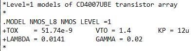
Calculations for Nmos Model:
Assume l = 5um and w = 500um, lets find parameters: VTO, GAMMA, KP, LAMBDA, and TOX
VTO
By observation of the data measured in part 1 VTO = 1.4V, while data measured in part 2 and VGS is at 3V IDsat can bee seen as approximately IDsat = 1.57mA
KP
Kpn = ID*2*(L/W)/(VGS-VTO)^2 = 1.57mA*2*0.01/(1.6)^2 then KPn = 12.26uA
Lambda
Lambda = slope/IDsat where slope = (1.6541mA - 1.57mA)/(5-1.5) = 0.02208mA/V. Then Lambda = 0.01406/V
TOX
tox = Eox/C'ox where Eox = Er*Eo = 3.9*8.85*10^(-18)F/um = 3.4515*10^(-17)F/um
where C'ox = 15pF/(5*500*10^(-12)) =
0.667fF/um^2 , here we used 15pF for Cox from the datasheet of
CD4007UBE.
resulting in tox = 51.74nm
GAMMA
g = sqr(2*q*Es*NA)/sqr(C'ox) = sqr(0.000496768) then gamma = 0.0222V
| VTO | 1.4V |
| KP | 12.26uA |
| LAMBDA | 0.0141V |
| TOX | 51.74nm |
| GAMMA | 0.02V |
| ID | 1.57mA |
Created Model:
NMOS device simulations:
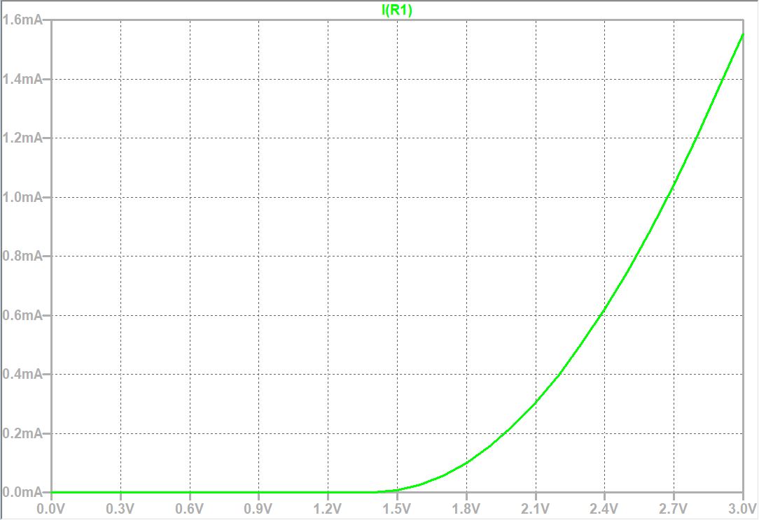
1. ID v. VGS (0<VGS<3V) with VDS = 3V
When
comepared to experimental results the plots are similar. Both sims and
experimental share the same VTO, however the sims reach 1.57mA at 3V
while the experimental reach 1.62mA at 3V. Also I should have gone in
0.5 increments of voltage in the experimental testing to ensure a
smoother curve for comparison.
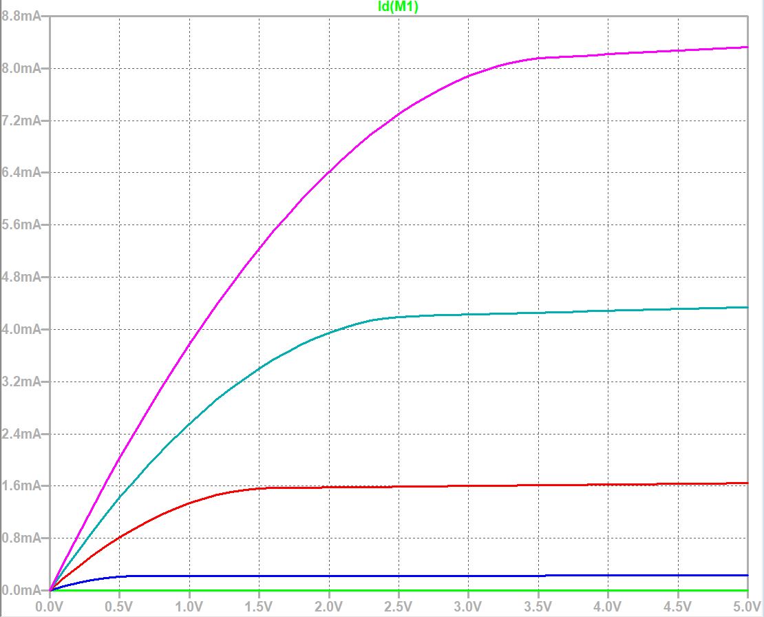
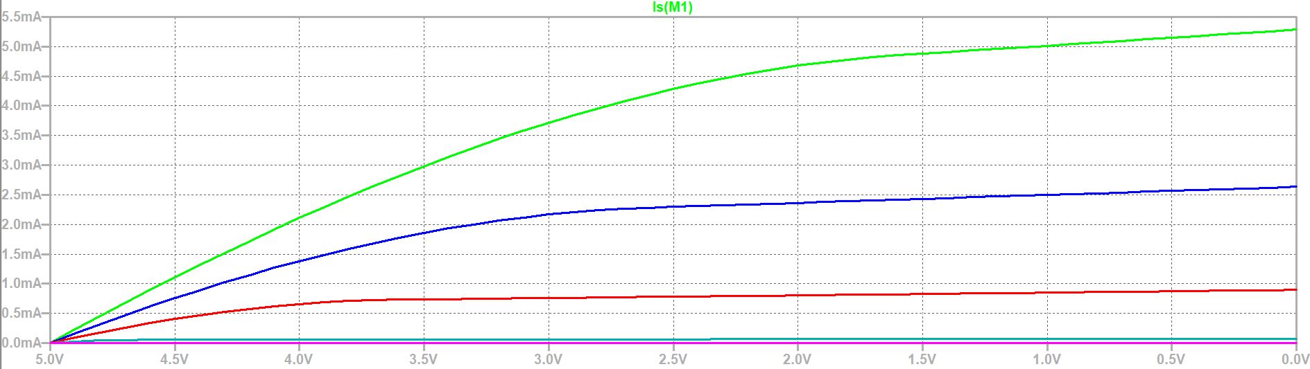
2. ID v. VDS(0<VDS<5V) with VGS varying from 1 to 5V in 1V steps.
GREEN:
VGS = 1V BLUE: VGS =2V RED: VGS
=3V TEAL: VGS = 4V PURPLE: VGS = 5V
The
experimental results at VGS =3V and simulations both begin to saturate
at approx 1.6mA, verifying the correct simulation model operation.
However the are some errors with higher VDS. Notice the simulations
reach 8mA while the experimental results only ream 6mA at VGS =5V
3. ID v. VGS(0<VGS<5) with VDS = 5V for VSB varying from 0 to 3V in 1V steps
GREEN: VSB = 0V BLUE: VSB = 1V RED: VSB = 2V TEAL: VSB = 3V
The
simulations wave form matches the experimental forms, however it seems
as if the simulations reachs higher ID more quickly. For example at VSB
= 0V ID=2mA when VGS = 3V in simulations, while experimentally
ID=0.83mA when VGS = 3V.
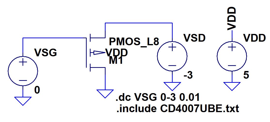
Part 2: PMOS device plots:
1. ID v. VSG (0<VSG<3V) with VSD = 3V
For
this circuit operations, the source (pin2) will see 3V and the drain
(pin1) will be grounded. Additionally the gate (pin3) will see the
variation from 0-3V.
Note the current is scaled to mA.
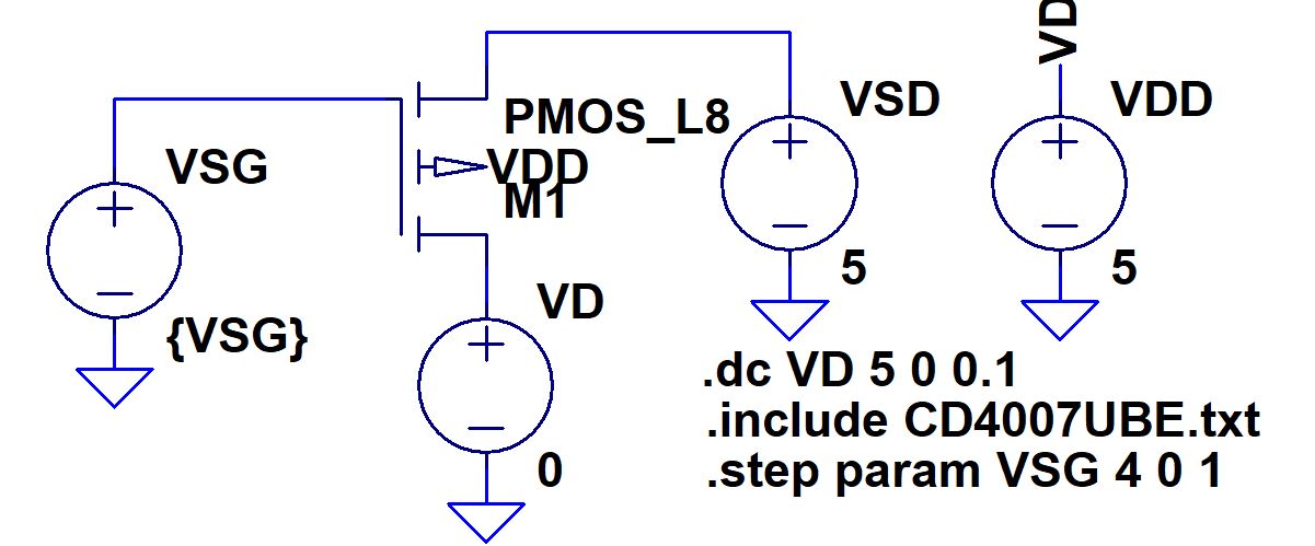
2. ID v. VSD(0<VSD<5V) with VSG varying from 1 to 5V in 1V steps
The first plot is essentially a flat line, but because the scale of the yaxis is so small it seems like a large jump.
Calculations for Pmos Model:
Assume l = 5um and w = 500um, lets find parameters: VTO, GAMMA, KP, LAMBDA, and TOX
VTO
By observation of the data measured in part 1 VTO = -1.6V, while data measured in part 2 and VSG is at 3V IDsat can bee seen as approximately IDsat = 0.87mA
KP
Kpn = ID*2*(L/W)/(VGS-VTO)^2 = 0.87mA*2*0.01/(1.6)^2 then KPn = 6.8uA
Lambda
Lambda = slope/IDsat where slope = (1.05mA - 0.87mA)/(5-2) = 0.06mA/V. Then Lambda = 0.069/V
TOX
tox = Eox/C'ox where Eox = Er*Eo = 3.9*8.85*10^(-18)F/um = 3.4515*10^(-17)F/um
where C'ox = 15pF/(5*500*10^(-12)) =
0.667fF/um^2 ,
here we used 15pF for Cox from the datasheet of CD4007UBE.
resulting in tox = 51.74nm
GAMMA
g = sqr(2*q*Es*NA)/sqr(C'ox) = sqr(0.000496768) then gamma = 0.0222V
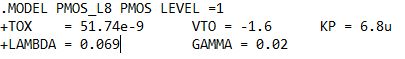
| VTO | -1.6V |
| KP | 6.8uA |
| LAMBDA | 0.069/V |
| TOX | 51.74nm |
| GAMMA | 0.22V |
| ID | 0.87mA |
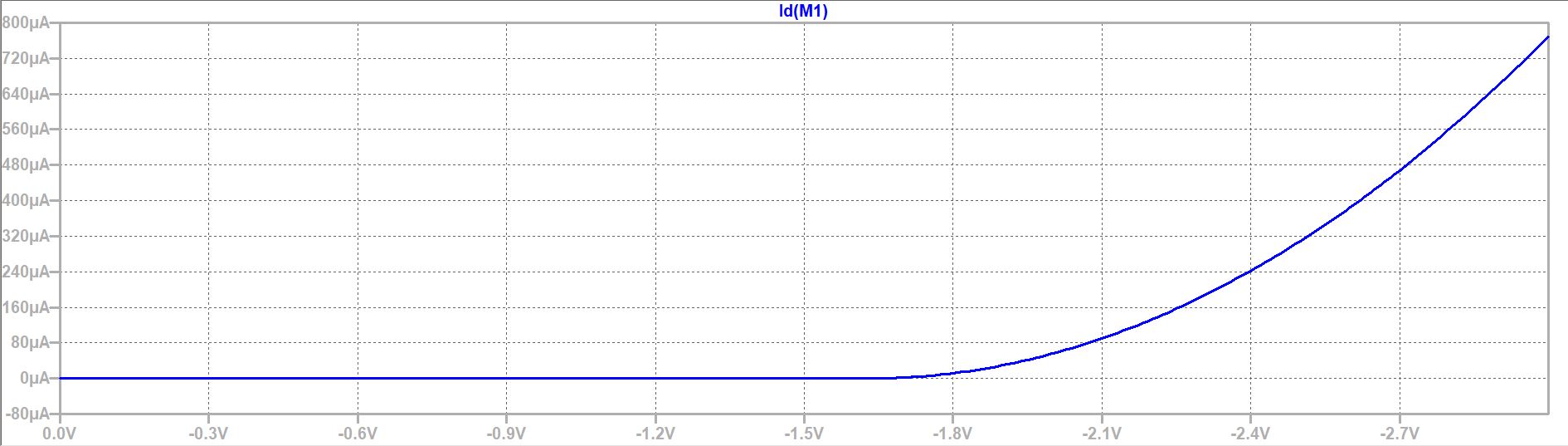
PMOS device simulations:
1. ID v. VSG(0<VSG<3V) with VSD = 3V
2. ID v. VSD(0<VSD<5V) with VSG varying from 1 to 5V in 1V steps
PURPLE
= 1VSG TEAL = 2VSG RED =
3VSG BLUE = 4VSG GREEN = 5VSG
We
can see that the threshold voltage may be too high, we know from
experimental results because VSG = 2 should have at least some current.
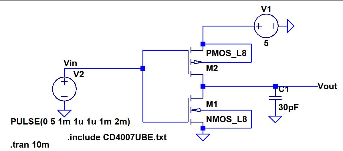
Inverter Using CD4007UBE
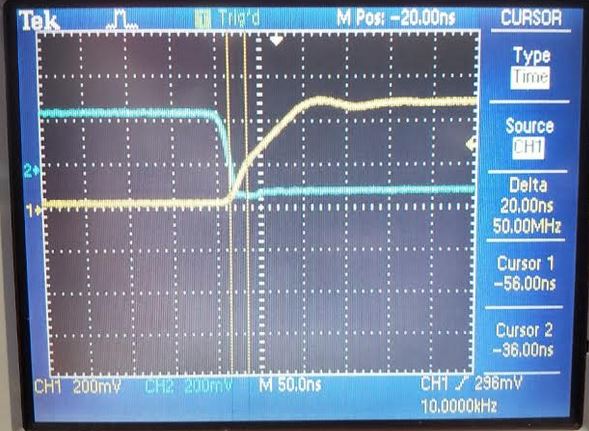
Experimentaly:
The delay through this inverter is approximatley 22nS.
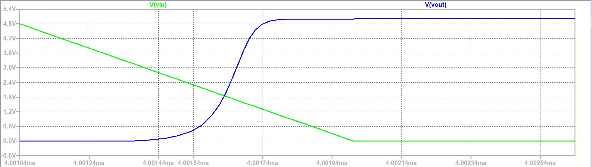
Simulations:
To measure the delay we move the cursors to 2.5V and look at the time
Vout = 4.00165ms Vin = 4.00149
Delay = 16nS
| Experiment Delay | Simulations Delay |
| 22nS | 16nS |
Return to butlerk2 EE 420L Reports
Return to EE 420L Labs