Lab 6 - ECE 420L
Authored
by Kyle Butler, butlerk2@unlv.nevada.edu
3/27/2019
Pre-lab work:
- This lab will utilize the ZVN3306A and ZVP3306A MOSFETs.
- Review these datasheets and become familiar with these transistors.
- Verify
that the simulations seen in lab6_sims.zip reasonably model the
behavior of the transistors' ID v. VGS, ID v. VDS, and gm v. VGS
curvers.
- Finally, watch the video single_stage_amps and review single_stage_amps.pdf
Lab work:
- Below are schematics for NMOS and PMOS source followers amplifiers (also known as common-drain amplifiers)
- In you lab report discuss the operation of these circuits.
- Simulate the operatioin of these amplifiers.
- Hand
calculate, and then verify your hand calculations with experimentation
and simulations, the gains and the input and output resistances
ensuring that your test signals are at a high enough frequency that the
caps have negligible impedance but not so high that the gain is
dropping off.
- If
you build this circuit using electrolitic capacitors, assuming
the
input AC signal swings around ground, put the "+" terminal of the cap
on the gate of the MOSFET. Please indicate, in your lab report, that
you understand why the capacitor is connected this way.
- In your lab report discuss, in your own words, how to measure the input resistance.
- For
measuring the input resistance add
a resistor equal to the value you calculated
between the input voltage source and the amplifier.
- Measure
the peak AC current through
this added resistor by taking the difference in the peak AC voltages
across the
resistor (on one side is the input voltage signal and the other side is
the
connection to the amplifier's input capacitor) and then dividing by the
resistor's value.
- Measure
the peak AC voltage on the
input of the amplifier (the left side of the capacitor).
- Dividing
this peak AC voltage by the
peak AC current through the added resistor is the amplifier's input
resistance.
- Again,
in your lab report discuss how to measure the
output resistance.
- For
measuring the output resistance,
add a resistor equal to the value you calculated in series with a big
capacitor
(to avoid messing up the biasing) from the amplifiers output to
ground.
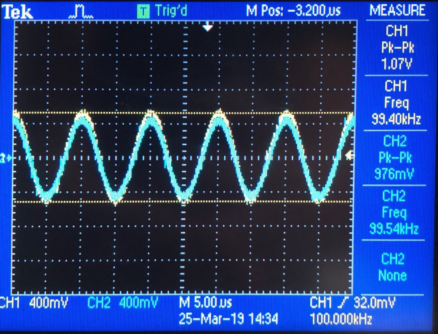
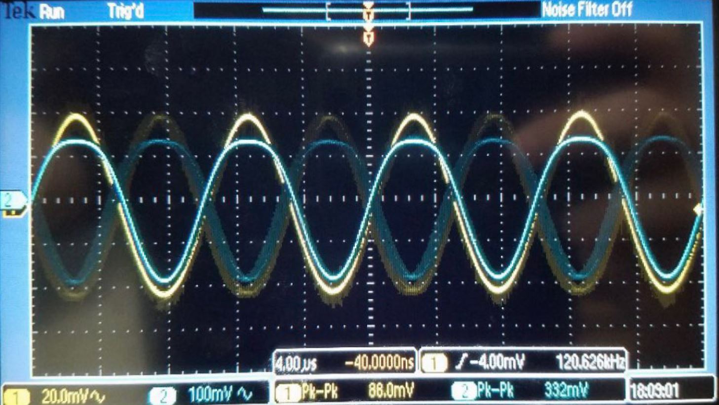
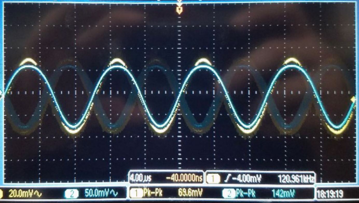
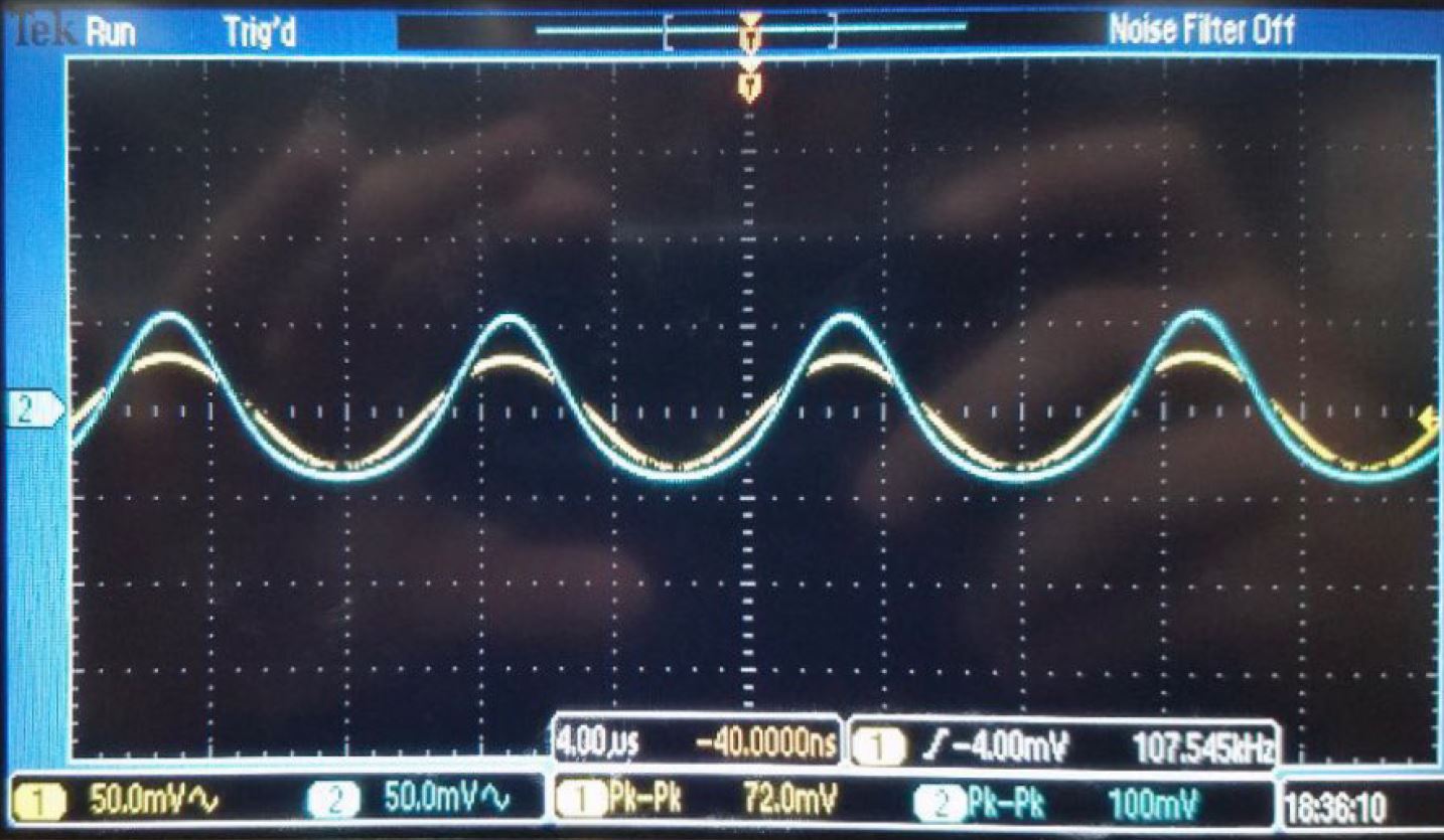
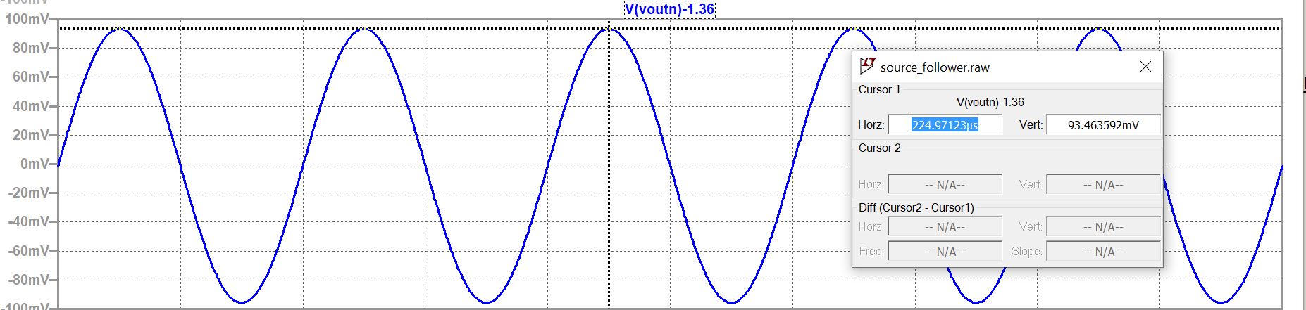
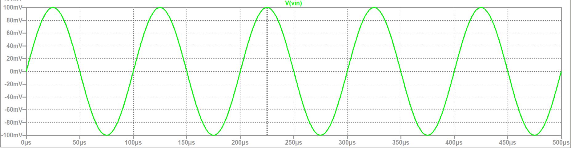
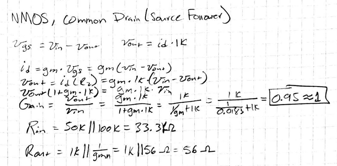
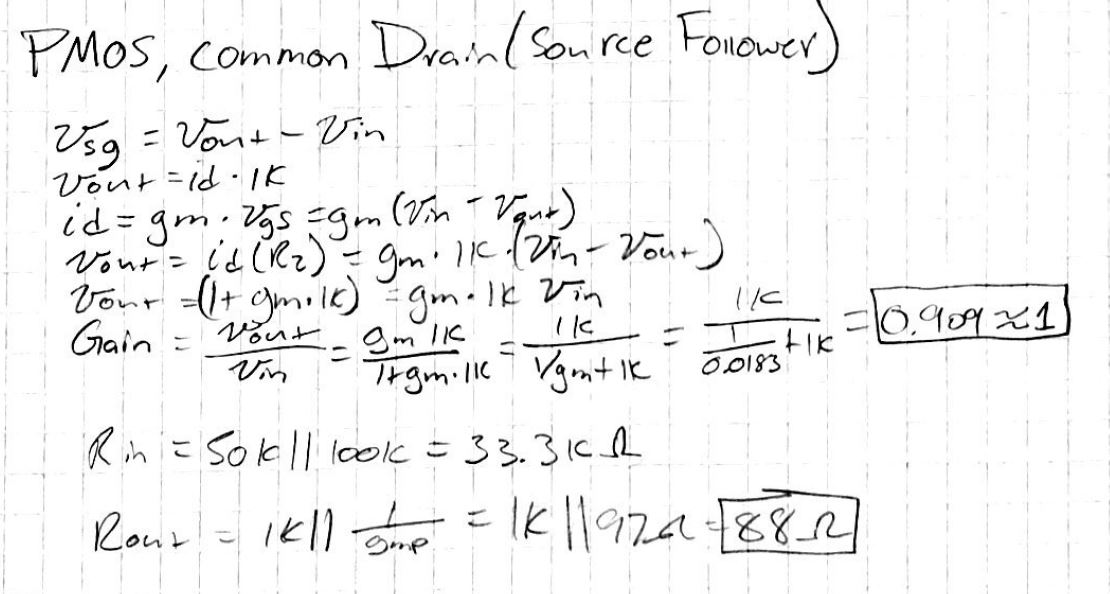
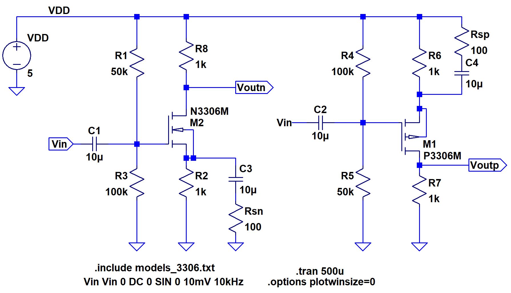
Part 1: Common Drain Amplifier
The
common drain amplifier is also known as the source followers amplifier.
This is because the expected gain is 1 and the output
'follows' the source. The drain is shared or common between the NMOS and PMOS giving the name common drain amplifier.
Schematic:
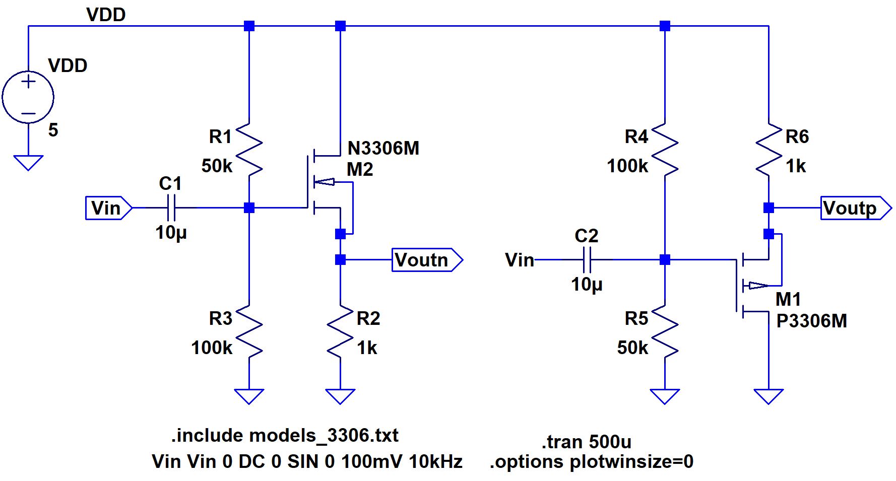
Simulations:
Circuit Operation
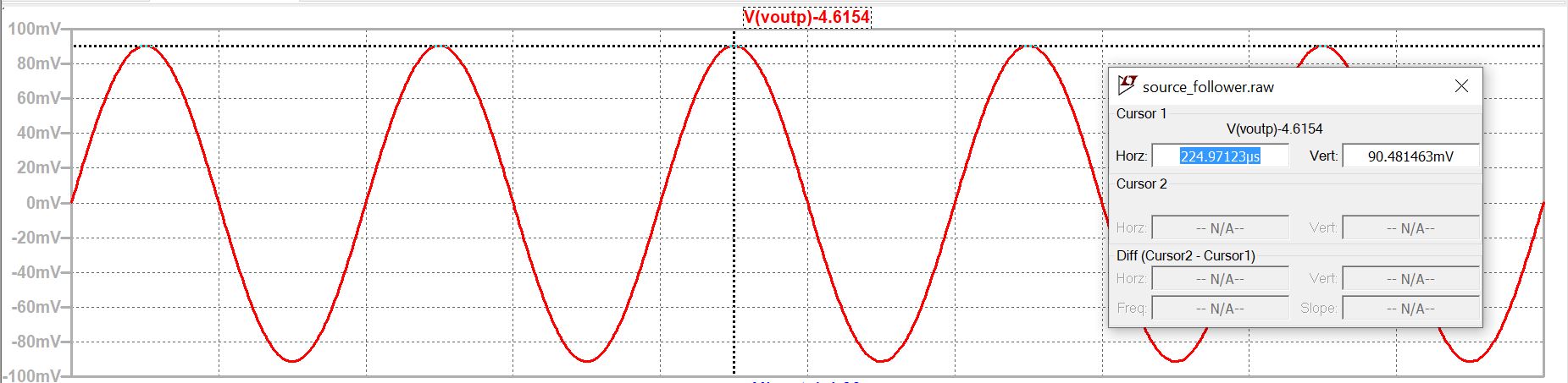
DC operation for hand calculations
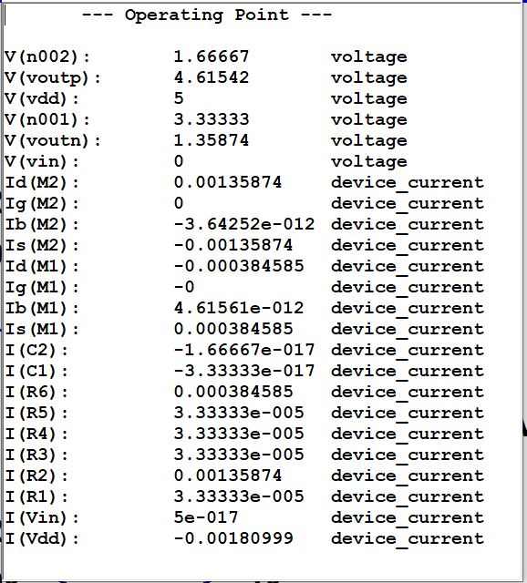
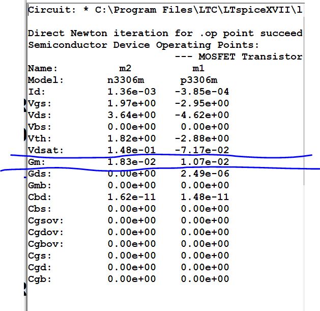
Hand Calculations:
When building the circuit we used electrolytic capacitors because those were the only type avaible in lab. As recommended
we
put the "+" terminal at the gate of the MOSFET. We did this because the
other orientation would cause a reverse the dielectric
insulation
separating the interior plates to breakdown. The AC voltage will cause
an unwanted chemical reaction unless the positive
terminal is connected to the higher potential DC voltage.
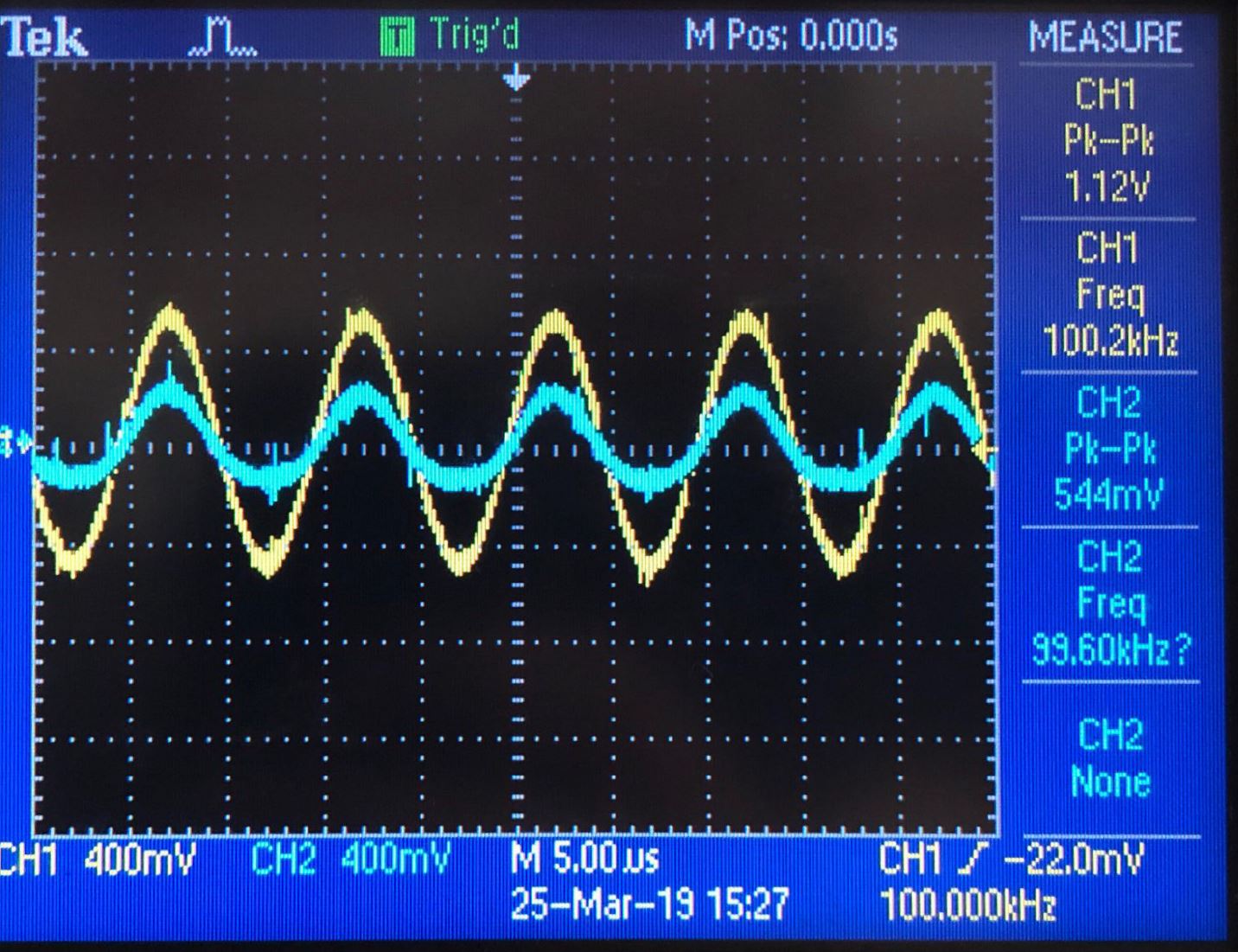
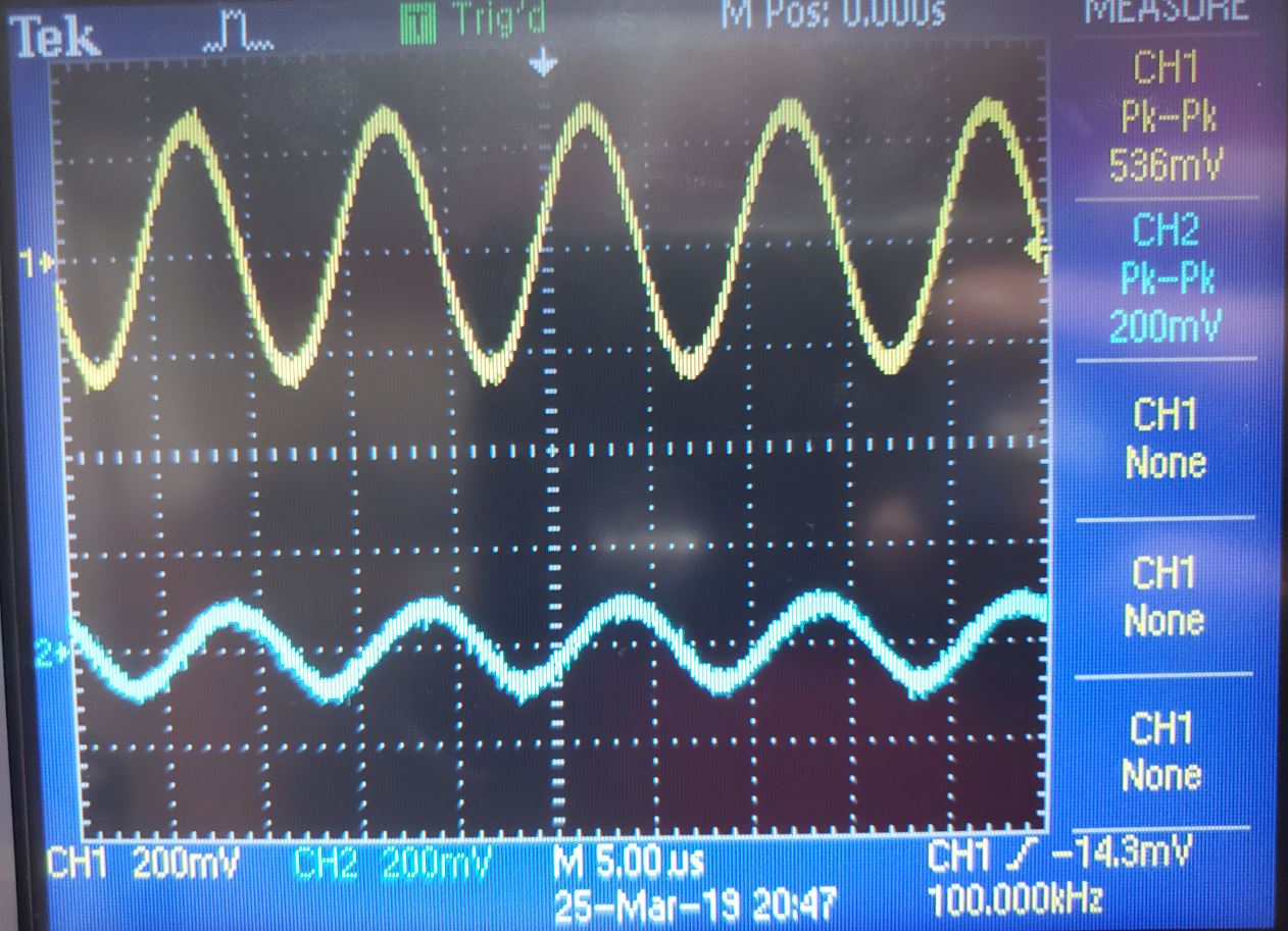
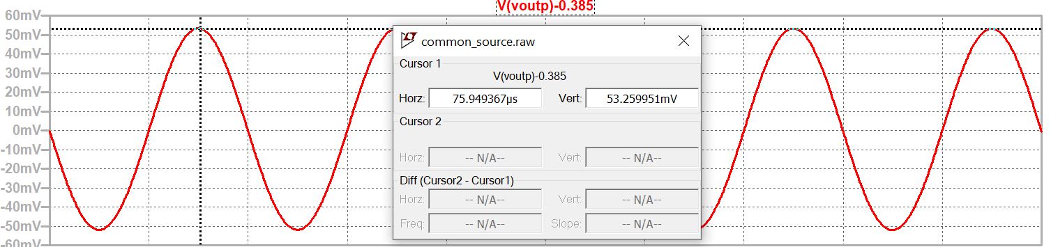
Experimental Results:
Summary:
| HAND | EXP |
| GAIN NMOS | 1V/V | 0.91 V/V |
| GAIN PMOS | 1V/V | 0.62 V/V |
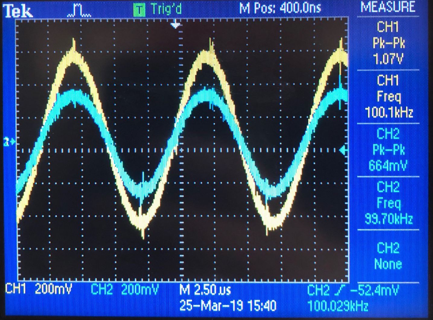
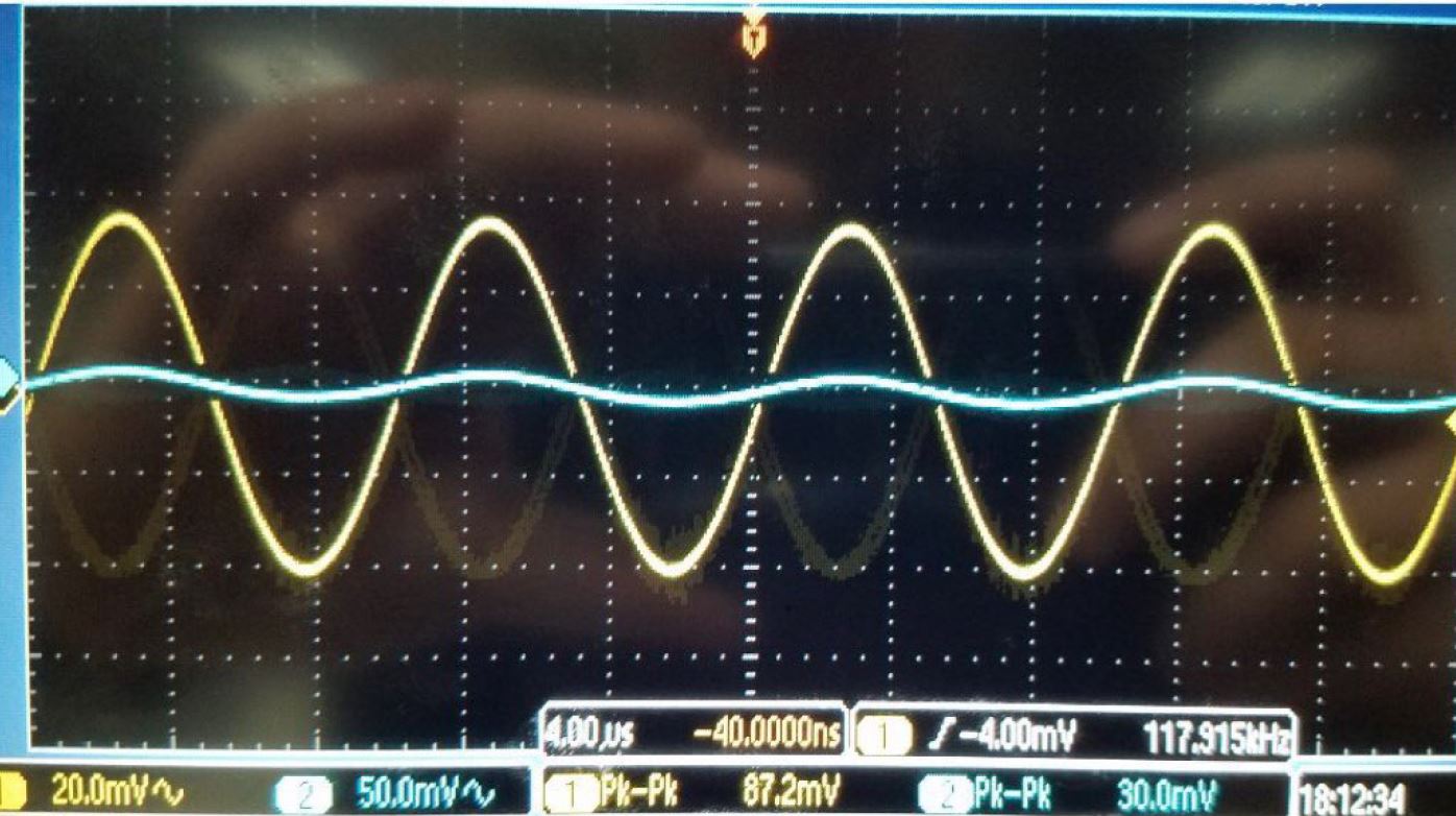
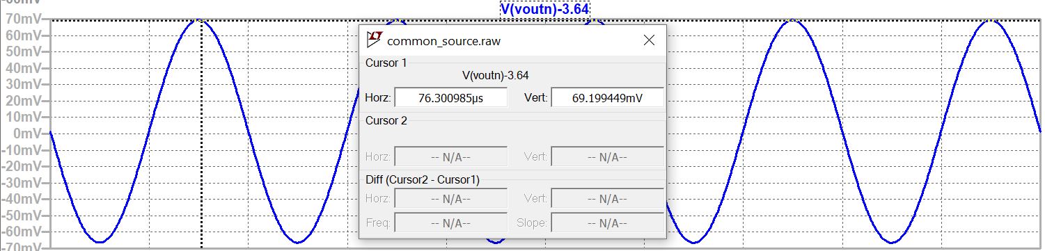
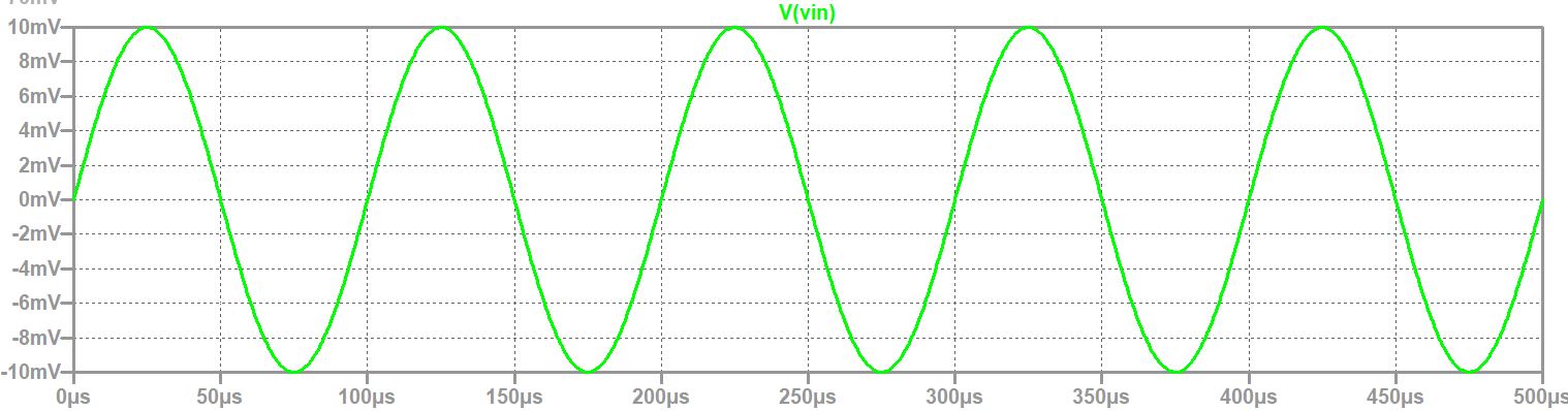
Part 2: Common Source Amplifier
Schematic:
Simulations:
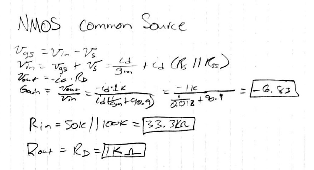
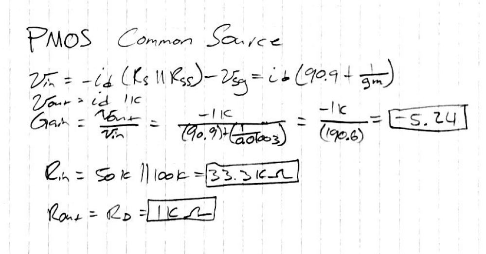
Hand Calculations:
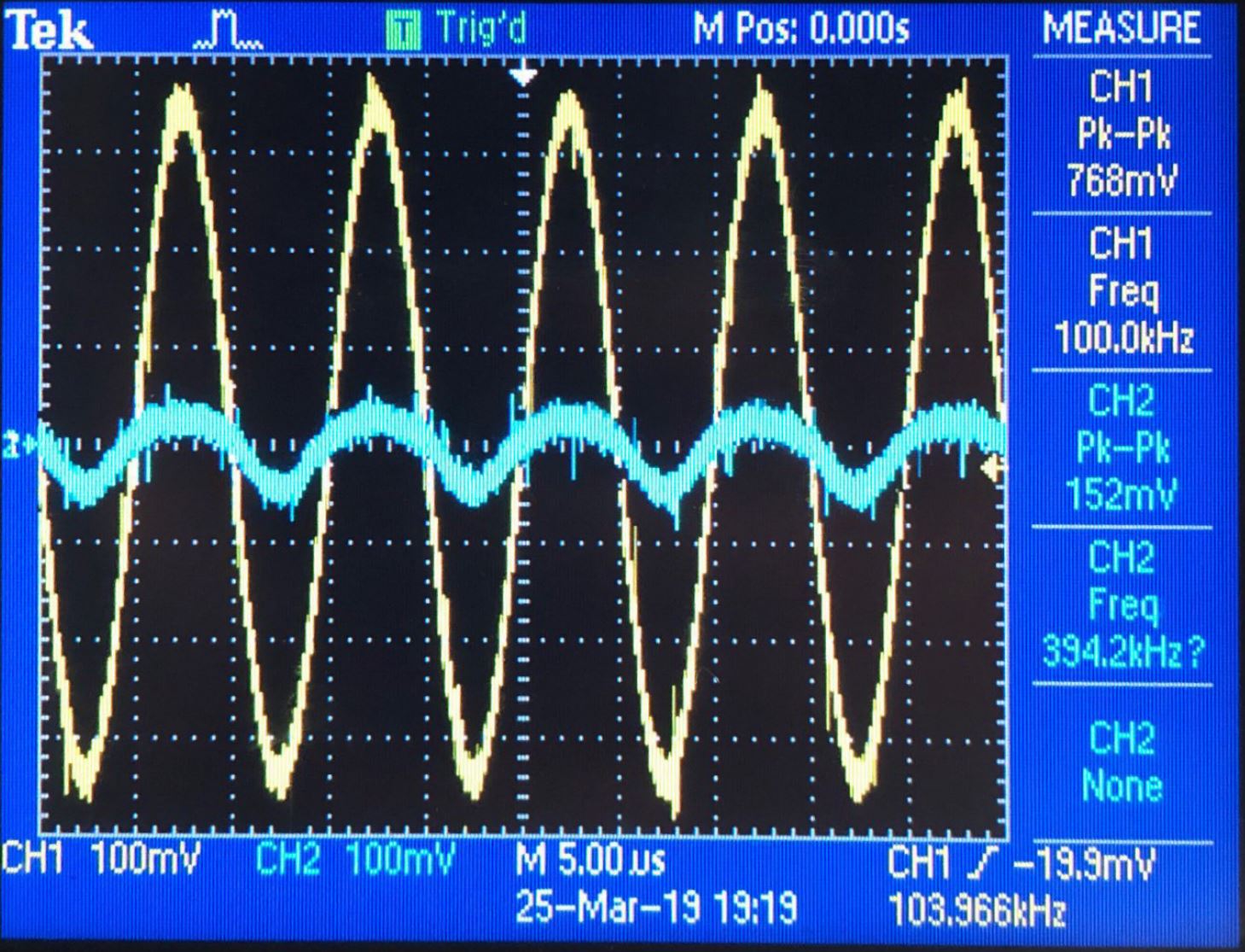
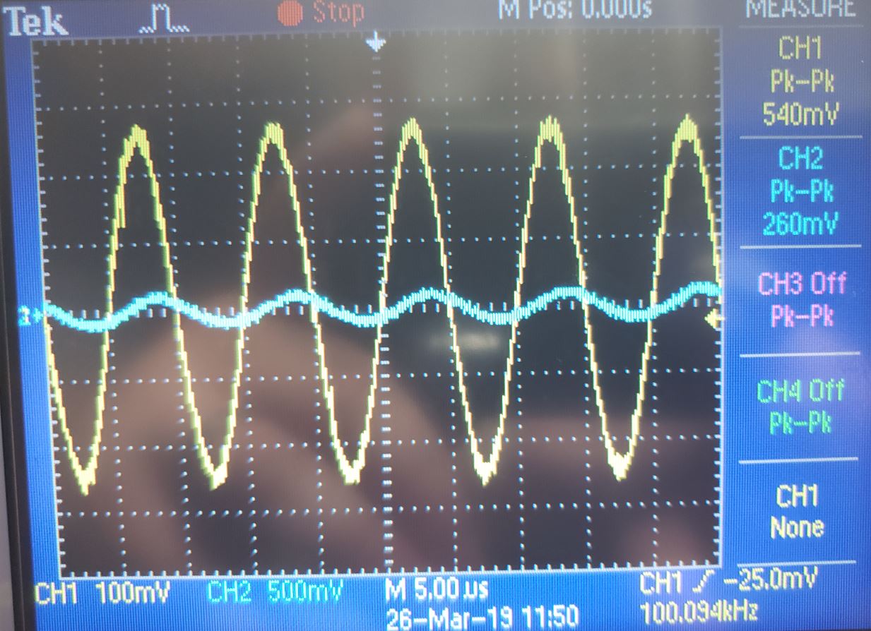
Experimental Results:
Summary:
| HAND | EXP |
| GAIN NMOS | 6.83V/V | 4.3V/V |
| GAIN PMOS | 5.24V/V | 3.08V/V |
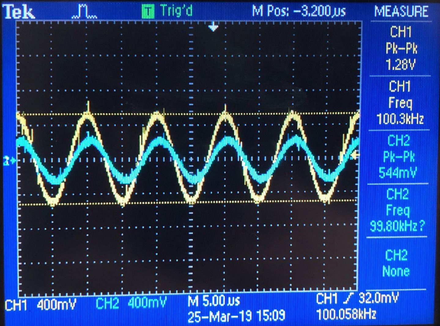
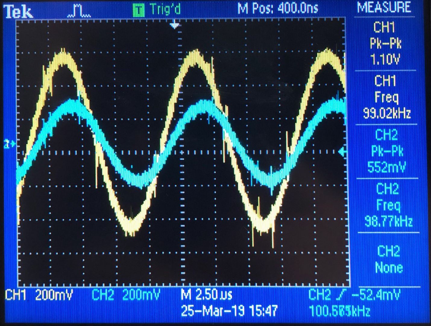
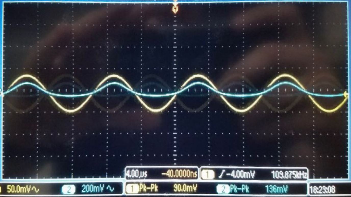
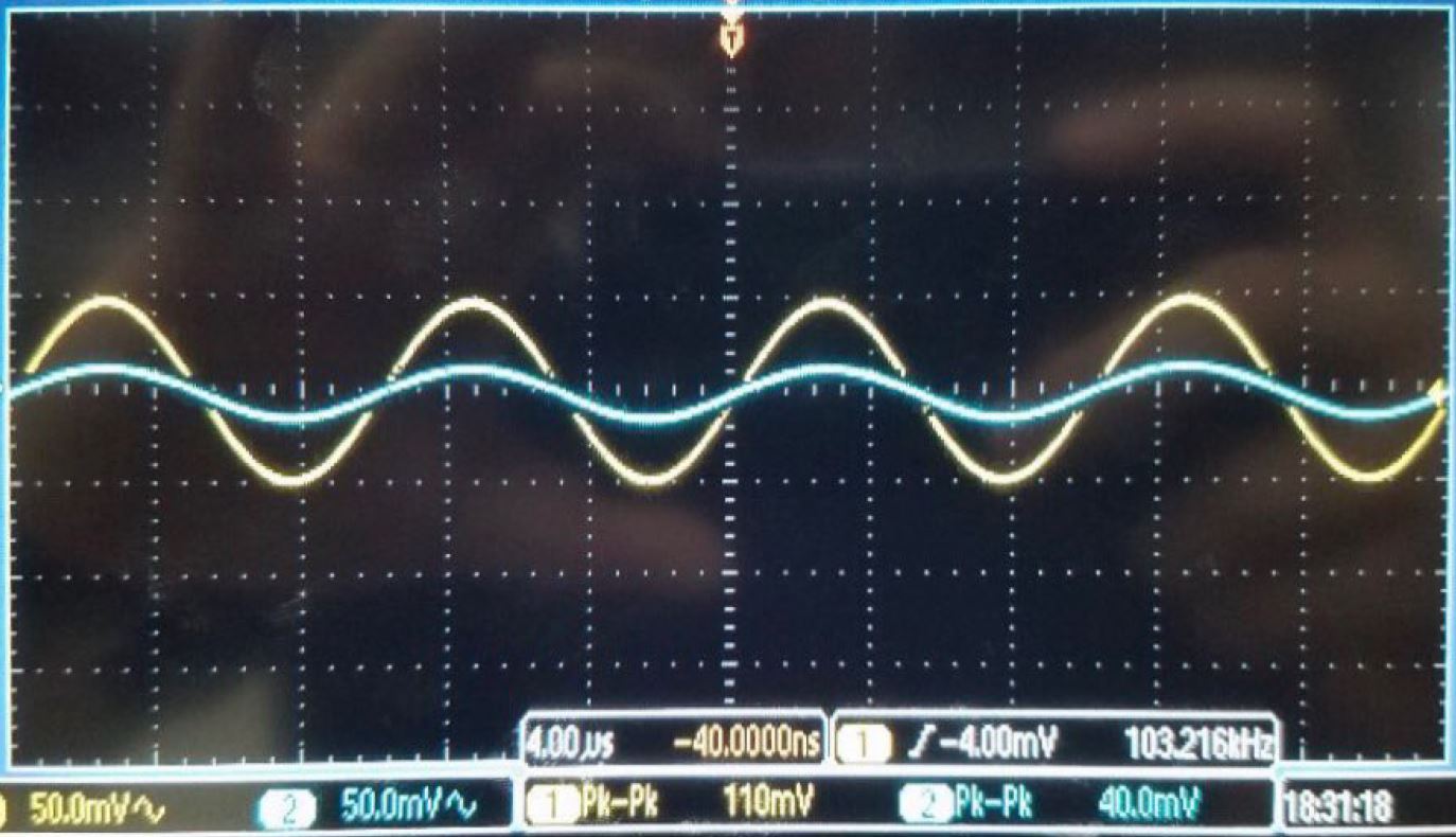
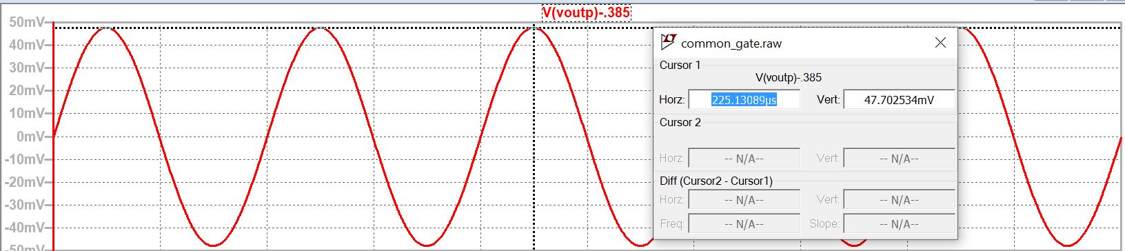
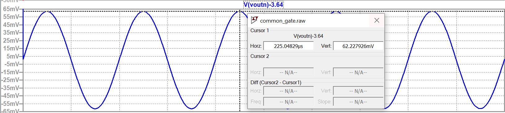
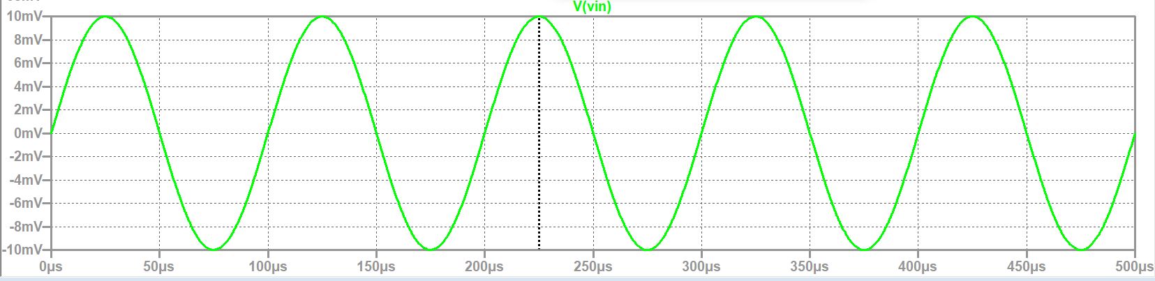
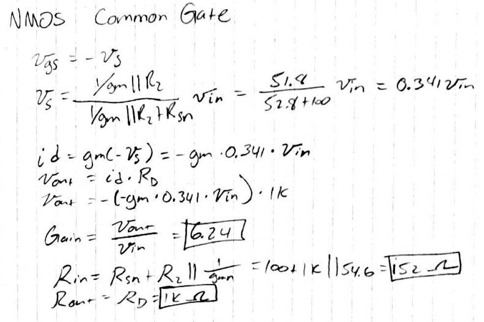
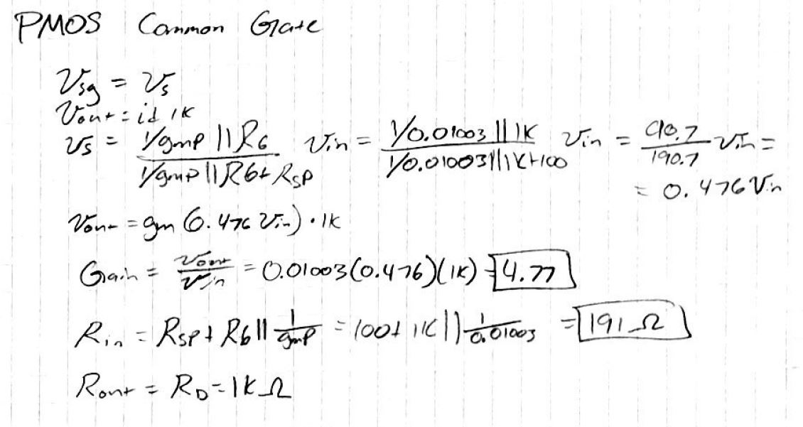
Part 3: Common Gate Amplifier
Schematic:
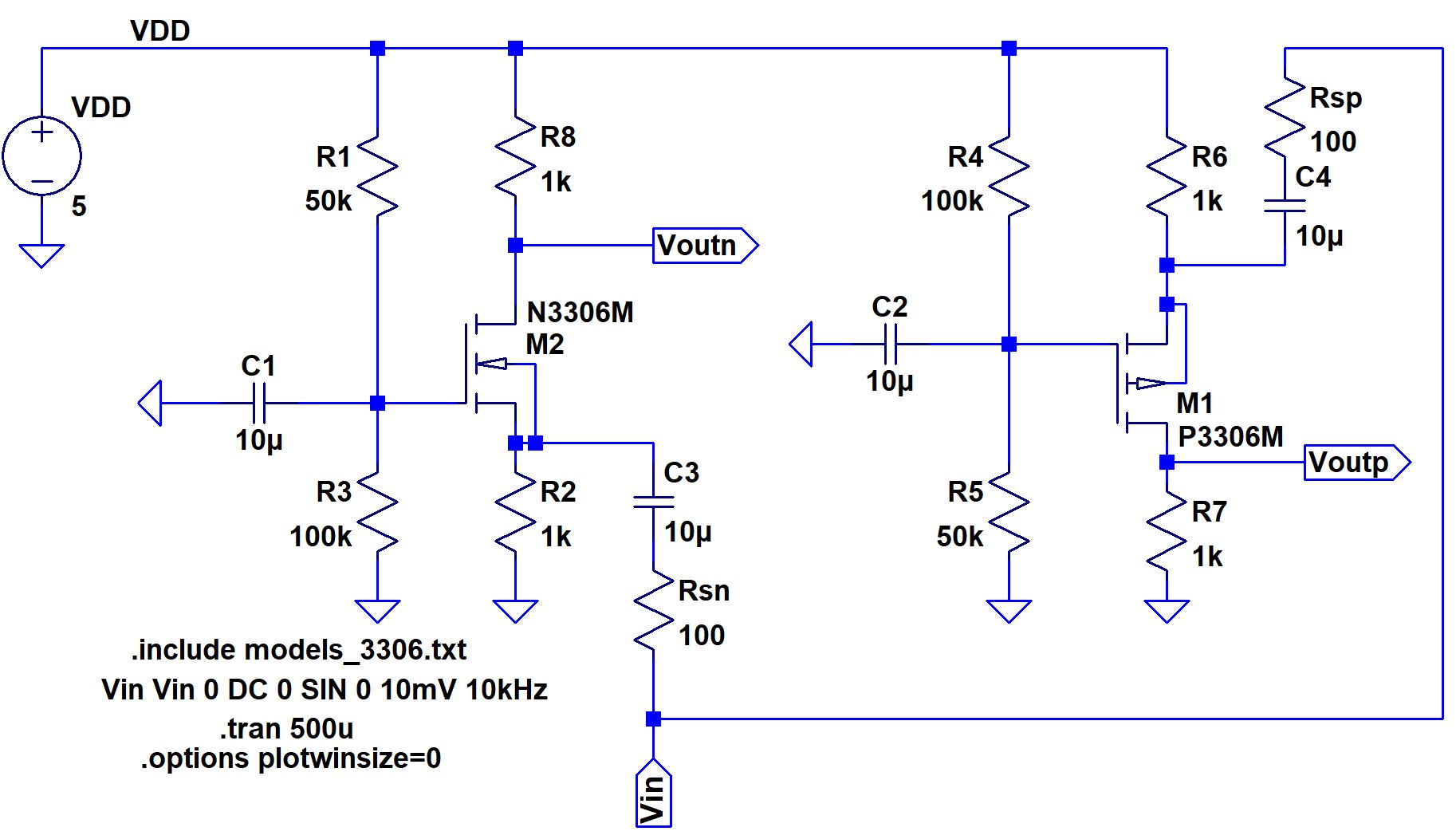
Simulations:
Hand Calculations:
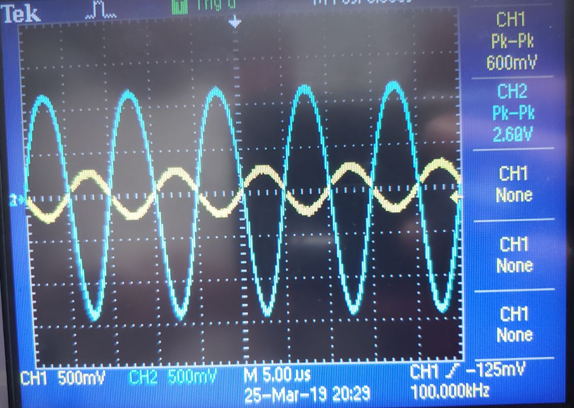
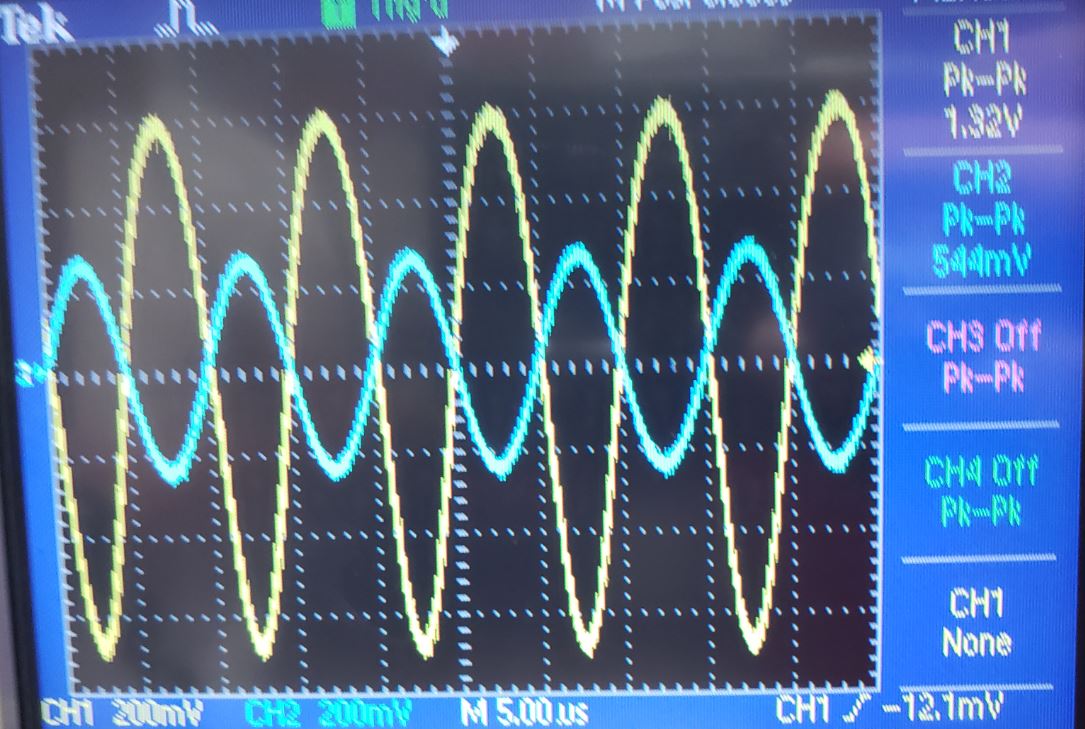
Experimental Results:
Summary:
| HAND | EXP |
| GAIN NMOS | 6.24V/V | 3.77V/V |
| GAIN PMOS | 4.77V/V | 1.5V/V |
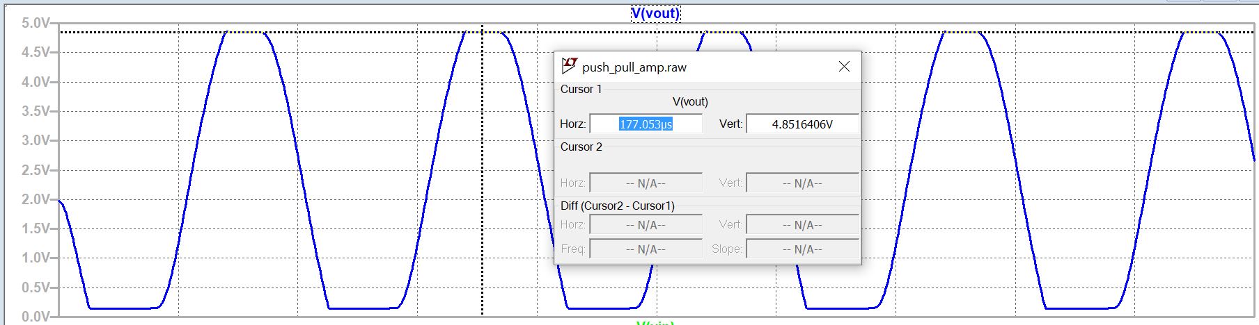
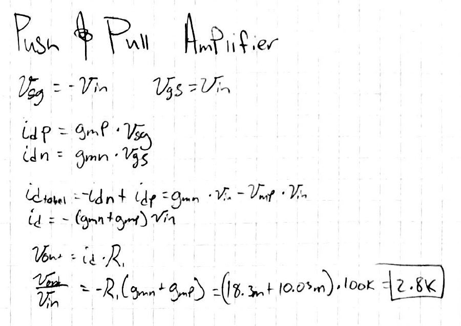
Part 4: Push Pull Amplifier
Schematic
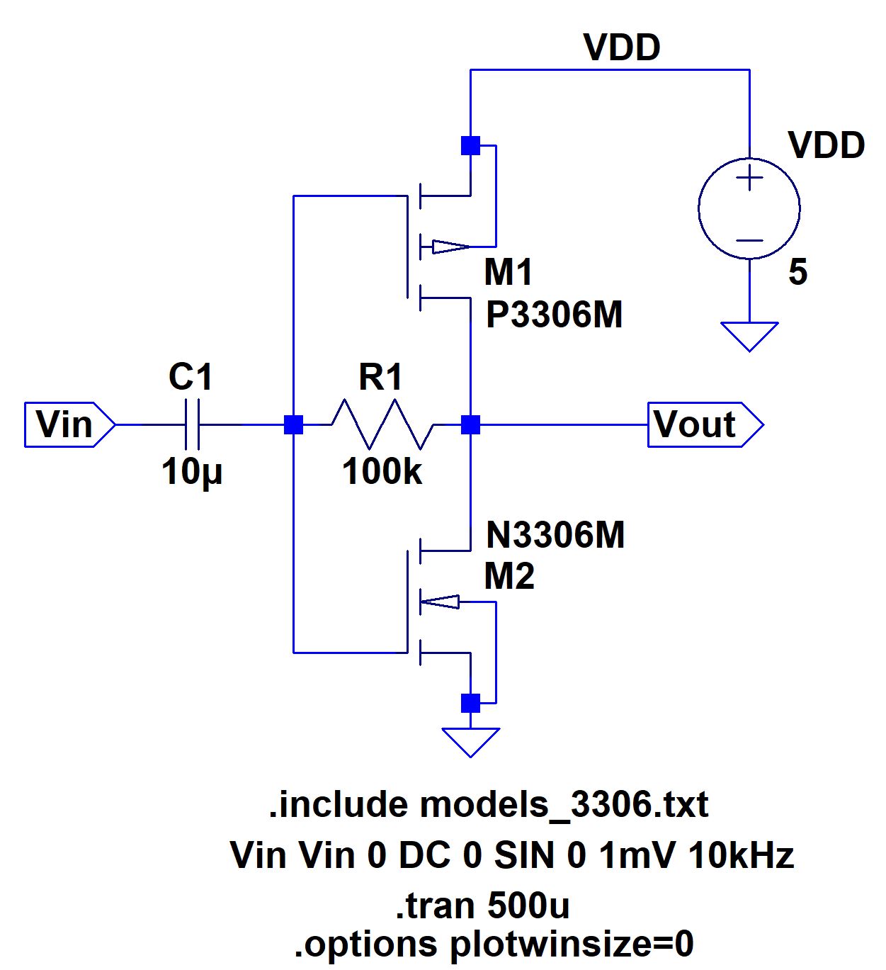
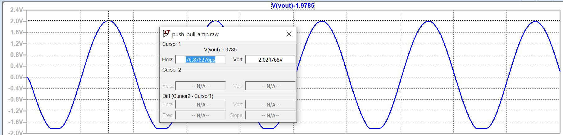
Simulations:
100k:
510k:
Do
you expect this amplifier to be good at sourcing/sinking current? Why
or why not?
Since at least one transistor is on at all times, the amplifier will be fine sourcing/sinking current.
What
happens to the gain if the 100k resistor is replaced with a 510k
resistor? Why?
The
gain is much larger with the 510k resistor because the transistor sees
a lower current. The gain is so much larger its hitting the rails.
Hand Calculations:
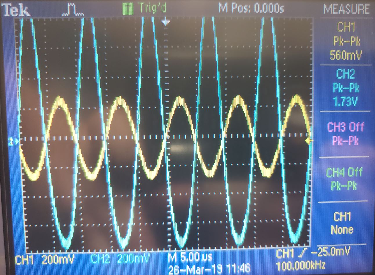
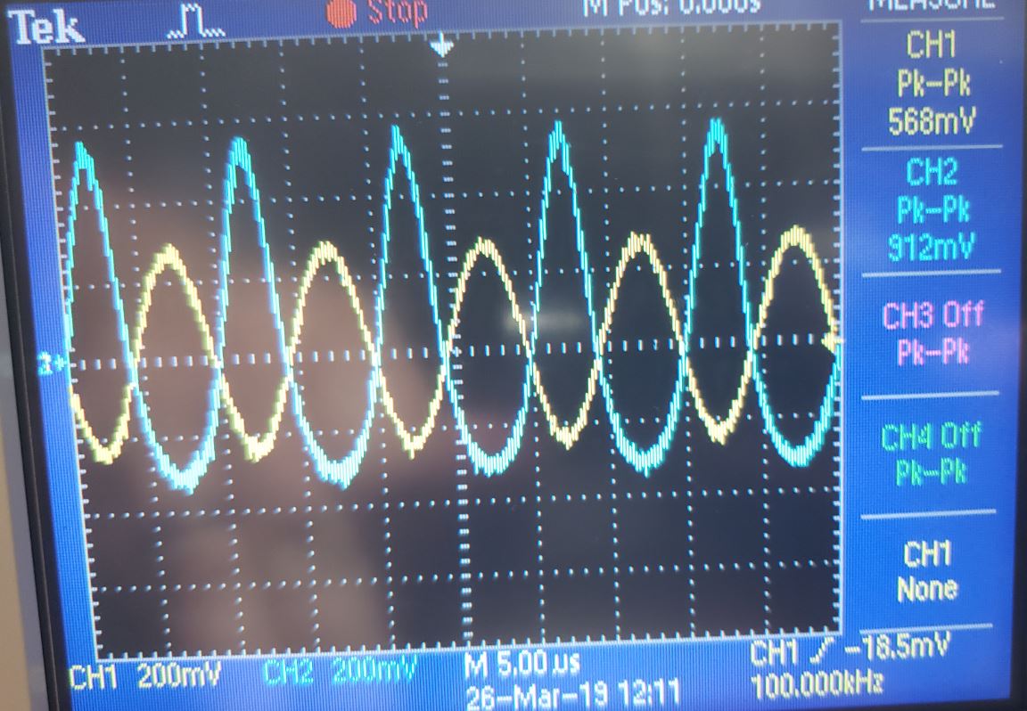
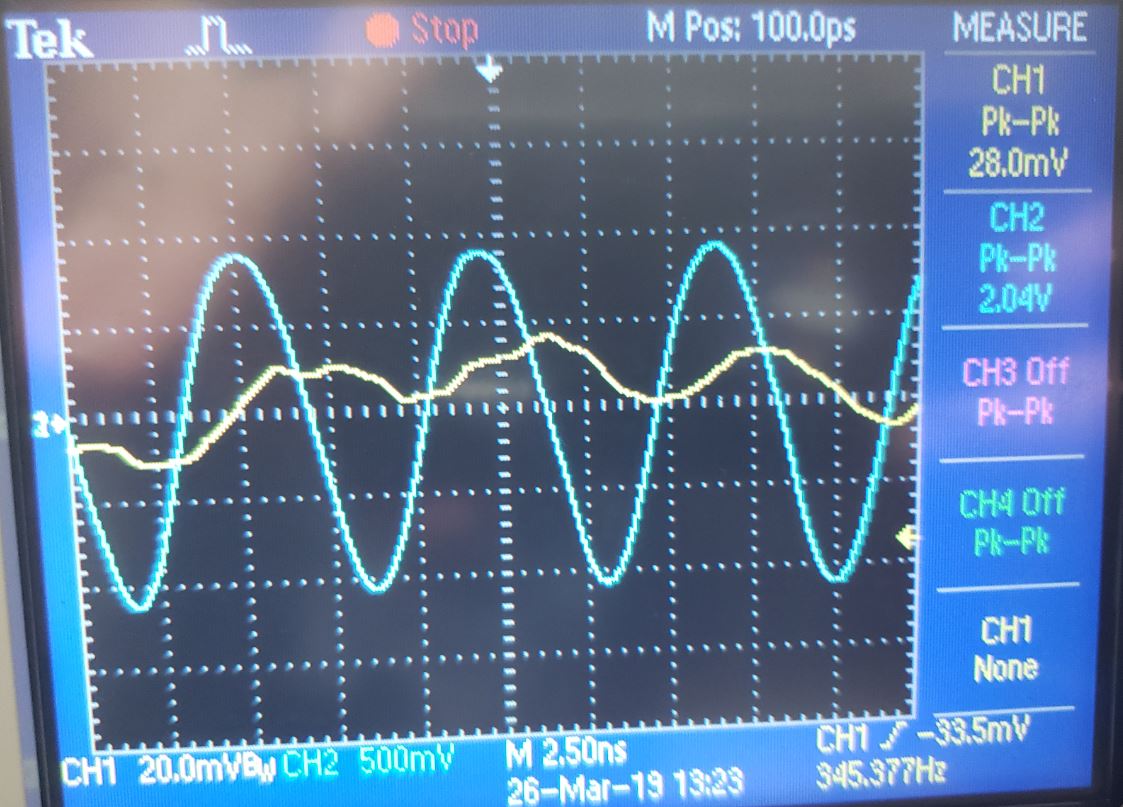
Experimental Results:
Summary:
| HAND | EXP |
| GAIN | 2.8KV/V | 2.04/0.028 = 72V/V |
Return to butlerk2 EE 420L Reports
Return to EE 420L Labs