Lab 3 - ECE 420L
Authored
by Kyle Butler, butlerk2@unlv.nevada.edu
2/20/2019
Pre-lab work:
- Watch the video provided and review the associated notes
- Read the write-up seen below before coming to lab
Lab work:
Introduction questions:
- This lab will utilize the LM324 op-amp, review the data sheet for this op-amp. For the following questions and experiments assume VCC+=+5V and VCC-=0V.
- Knowing the non-inverting input, Vp is at the same potential as the inverting input, Vm, (called the common-mode voltage, VCM) what are the maximum
and
minimum allowable common-mode voltages?
- The max common mode voltage is VCC-1.5V, so with VCC=5V the max common mode voltrage is 3.5V.
- What
is a good estimate for the op-amp's open-loop gain?
- With a supply voltage of 5V, the estimated gain is 115dB. Resulting in AOL=10^(115dB/20) = 526K
- What is a good estimate for the offset
voltage?
- From the datasheet the typical offset is 2mV, while worst case design offset is 9mV.
Build and test the circuit:
Real world
circuit
Real world measurement
Circuit
simulation
Measurement simulation
- What is the common-mode voltage, VCM? Does VCM change? Why
or why not?
- The
VCM is the voltage seen across the input terminals, which is 2.5V.
Since the inverting input is at ground and the non-inverting terminal
is 2.5V, the VCM must be 2.5V. This can be seen in both the real world
measurement and the simulation.
- What is the ideal closed-loop gain?
- Closed loop gain for inverting
orientation is -(Rf/Rin), since both resistors are 5k the resulting
closed loop gain is -1. This can be seen by the phase shift between Vin
and Vout in the measurement simulation.
- What is the output swing and what is it centered around?
Output Swing
Clipping- From the simulation measurements the output swing is 100mV, while the real world measurement is 111mV.
- Additionally
the output swing is centered around the DC offset or VCM of 2.5V, if it
is not centered around 2.5V it is possible for the output to reach the
maximum or minimum voltage of the rails. This causes clipping around 0V
and 5V.
- What is the maximum allowable input signal amplitude? Why?
- Considering
the VCM of 2.5V, the max input signal amplitude is 2.5V. Any larger
then 2.5V results in a clipping at the rails around 5V.
- What is the maximum allowable input signal if the magnitude
of the gain is increased to 10? Why?
- By
increasing the gain by factor of 10 the max allowable input signal must
reduce by a factor of 10. The max input signal with a gain of 10 is
250mV. The output will swing from 5V to 0V centered around VCM
- What is the point of the 0.01 uF capacitors from VCC and
VCM to ground?
- Similarly
to the reasoning of putting capacitors to ground on an Opamps supply
voltage, it is to reduce the noise or rippling of the voltage.
- The
0.01uF capacitors can be replace with 0.1uF-1000pF because it does not
effect the output voltage and the input signal is a DC source, no
filtering of ripple is neccessary.
- The data sheet shows that this op-amp has an input bias
current that flows out of the op-amp's inputs of typically 20 nA. This current flows out of both the non-inverting and
inverting inputs through the resistors connected to these inputs.
- Show how the operation of the circuit can be effected if,
for example, R1 and R2, are much larger. Explain what is going on.
- Since
the input bias current is small (20nA) and the resistor values used for
R1 and R2 are small we see a current in the range of 250uA, the input
bias is negligible when compared to the curent flowing in the
circuit.
- However, if the resister values were much larger, say by a factor of 1000, the
circuit flowing through the circuit will be in the nA range and the
input bias current effect will be observed in this current range.
- This
change in current will result in a change in VCM, leading to the
possiblilty of a clipping effect or at the very least a shift in the
output voltage.
Op-amp offset voltage:
- By
using the following circuit layout we can measure the offset voltage as
Vos=(VCM-Vout)/Gain. For the 4 different opamps the VCM will be 2.5V
and the Gain will be 20.
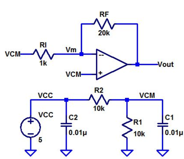
- The following Opamps used the same circuit layout as part 1, but with resistor values of 1k and 20k.
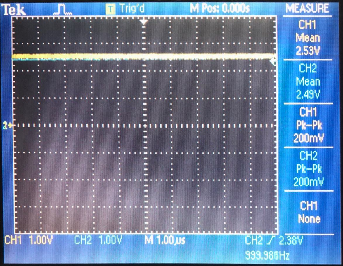
- LM324
- Vos = (2.53-2.49)/20 = 2mV
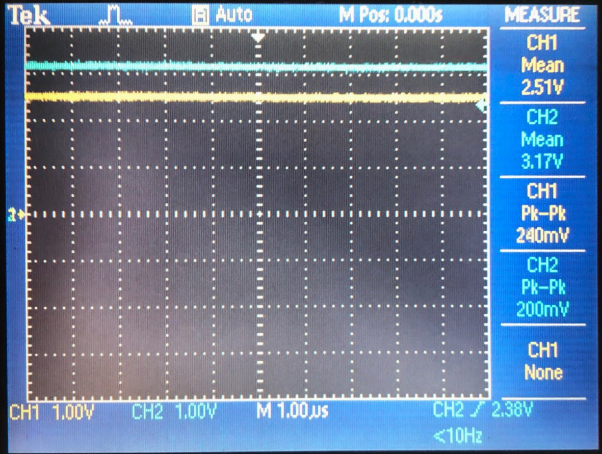
- LM348
- Vos = (2.51-3.17)/20 = -33mV
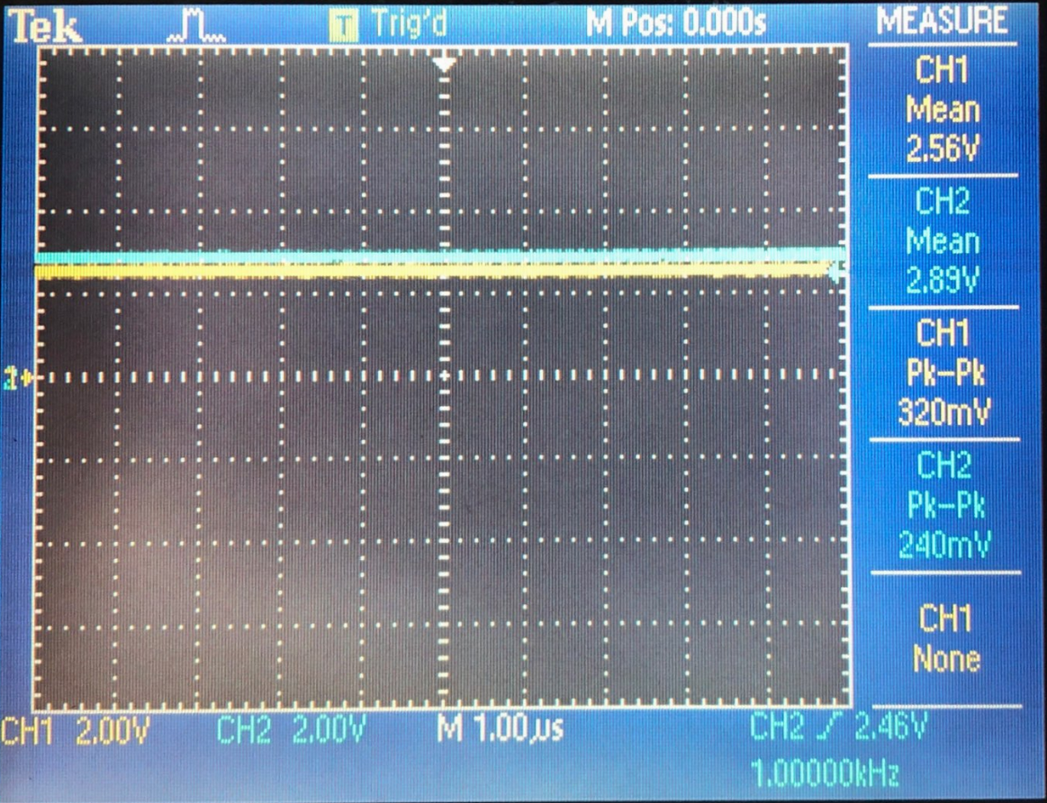
- LT(forgot number, get from lab later)
- Vos = (2.56-2.89)/20 = -16.5mV
- LM393
- Vos = (2.51-2.03)/20 = 24mV
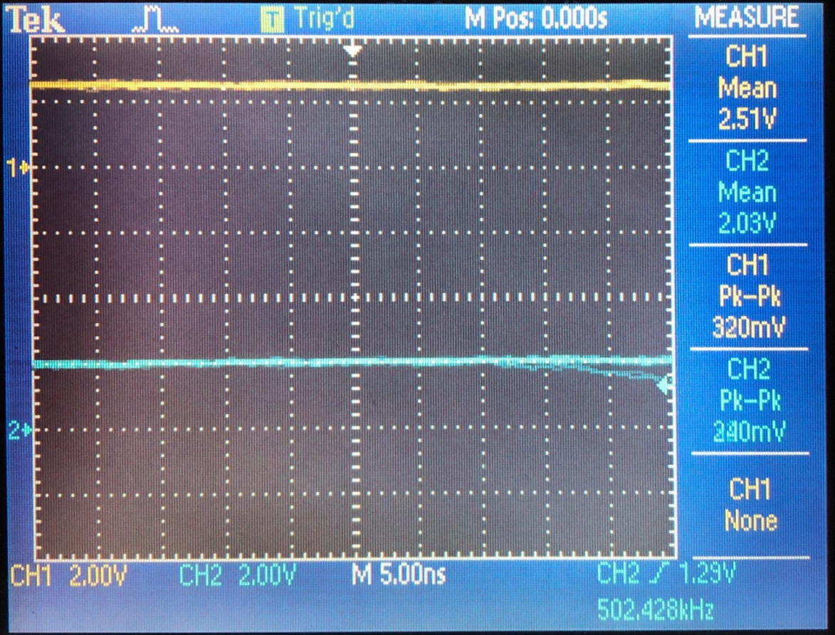
- The Opamps besides the LM324 had large offset voltages campared to the LM324. I
beleive we should have selected to use a larger gain (200)) for these
opamps and that our resistors values may have been effected from input
bias current.
Return to EE 420L Labs