Lab 1 - ECE 420L
Authored
by Kyle Butler, butlerk2@unlv.nevada.edu
1/30/2019
Pre-lab work:
- Prior to the first day of lab request a CMOSedu account using a UNLV email adress from Dr. Baker.
- Review the provided material regarding editing webpages in order to draft the lab report using html.
- Read the entire lab write-up before attending lab.
Lab work:
- Simulate,
and verify the simulation results with experimental measurements, the
circuits seen in Fig. 1.21, 1.22, 1.23, and 1.24 (use a 1uF cap in
place of 1pF cap). The figures can be found in CMOS Circuit Design,
Layout, and Simulation, Third Edition by Dr. Baker.
- For the AC
response seen in Fig. 1.23 generate a table showing some representative
measurement results (frquency, magnitude, and phase).
Provide the following
- Circuit
schematic showing values and simulation parameters (snip the image from
LTspice).
- Hand
calculations to detail the circuit's operation.
- Simulation
results using LTspice verifying hand calculations.
- Scope
waveforms verifying simulation results and hand calculations.
- Comments
on any differences or further potential testing that may be useful
(don't just give the results, discuss them).
Fig. 1.21 and
Fig. 1.23(AC Response
of Fig. 1.21)
Schematic and Simulation:

(A) Above is the Transient of Fig1.21/1.23 from LTspice
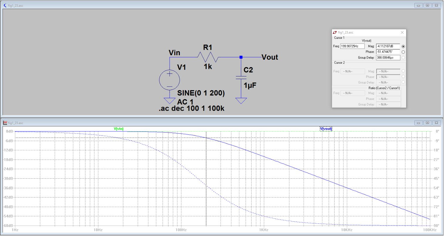
(B) Above is the AC response for Fig1.23 from LTspice with the measurement tool observing 200Hz.
Hand Calculations:
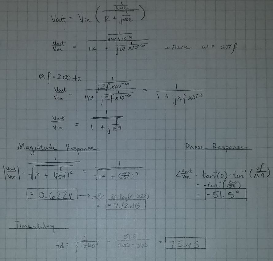
(C)
Above you can see that our calculated magnitude response of 0.622V or
-4.12dB matches the simulation of LTspice in image (A) for V and image
(B) for dB.
Additionally the phase response matches the simulated phase of LTspice seen in image (B). Now its time to build the circuit.
Circuit:
Unfortunately we did not have breadboards for Lab 1 and had to construct on off board circuit seen below.
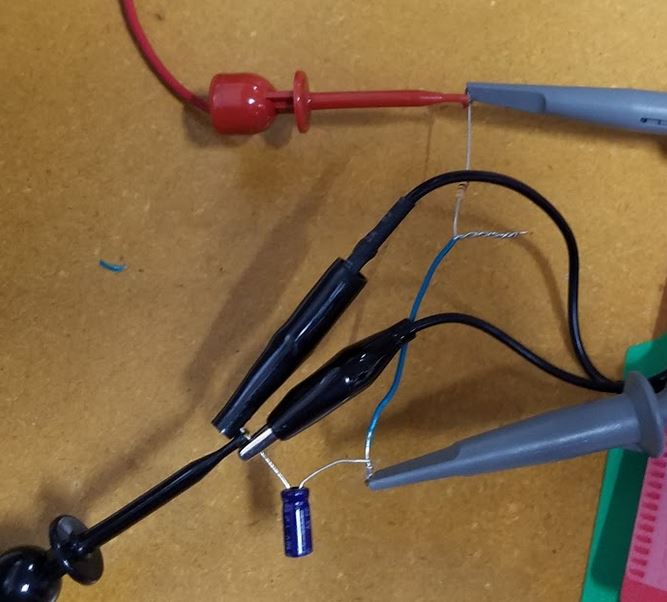
(D) The scope probe on the southside of the image is measureing the output, leaving the north probe measuring input.
Experimental measurements:
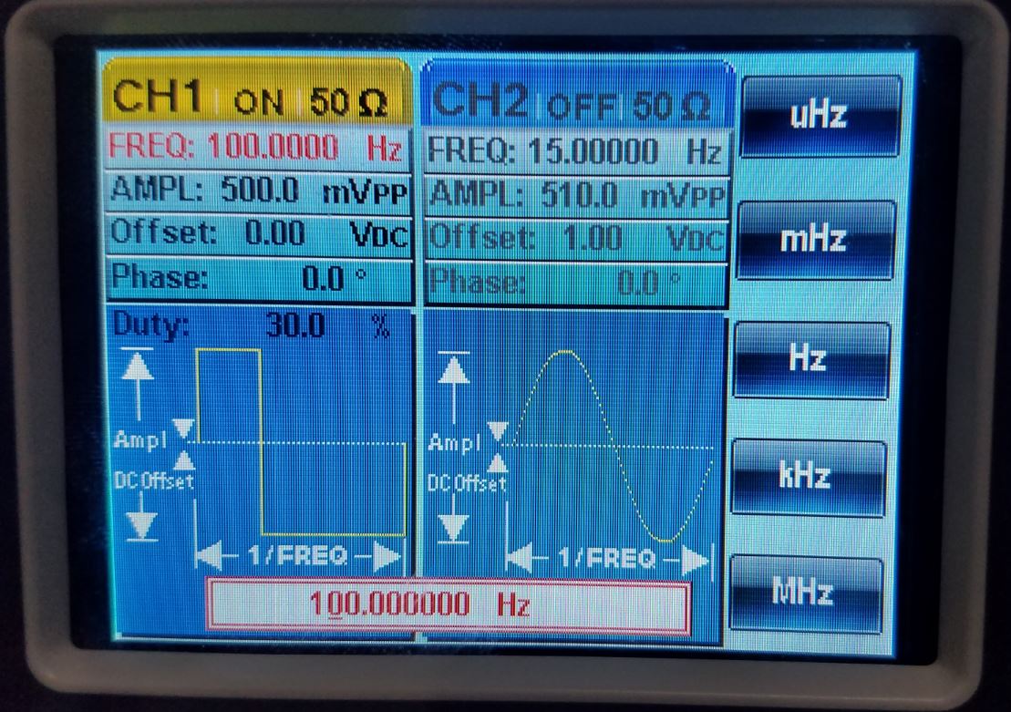
Input using frequency generator
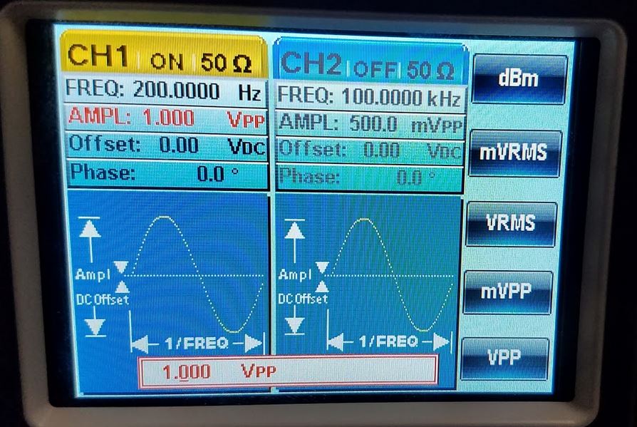

(E)
Magnitude and time delay of experimental circuit. We measure a voltage
of 0.64V at 500mV per square and a delay of approx. 700us. Next
lab we will use the cursors tool to measure
Now we will measure the AC response by inputing different frequencies.
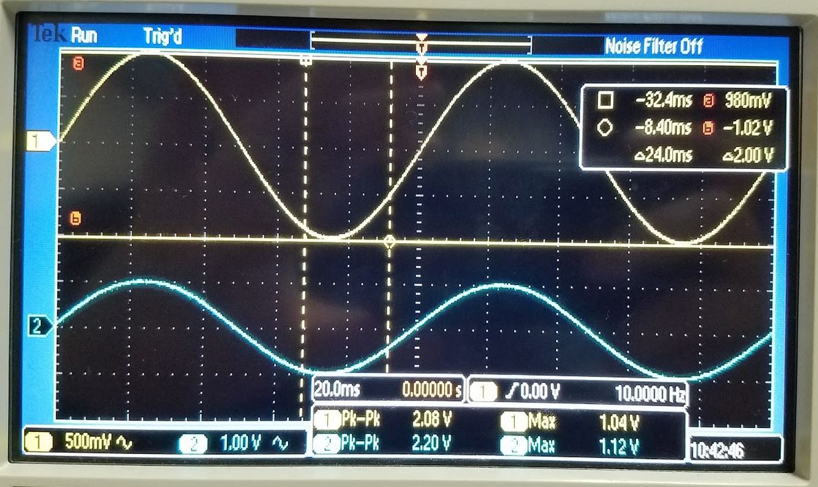
(F) 10 Hz
(G) 100Hz
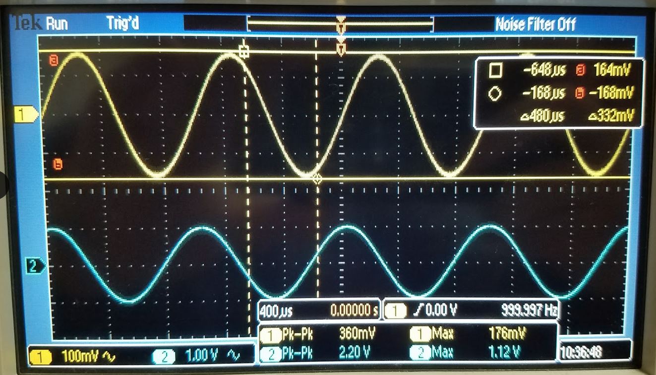
(H) 1KHz

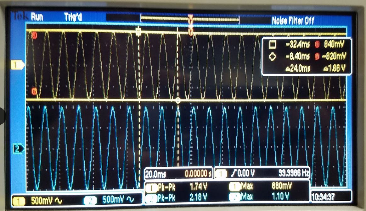
(I) 10KHz
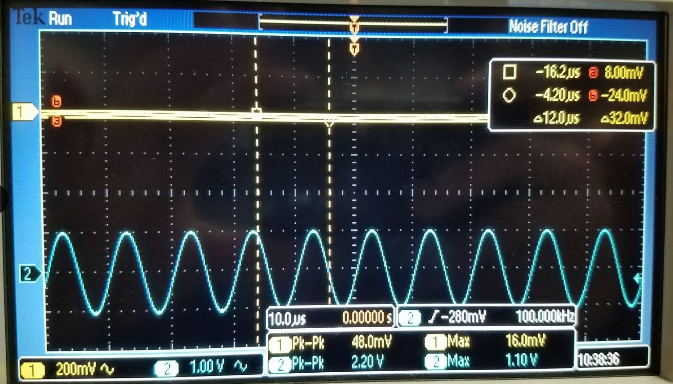
(J) 100Khz
(K) Below is the Table and Plot for the experimental measured values
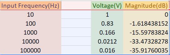

Fig. 1.22
Schematic and Simulation:
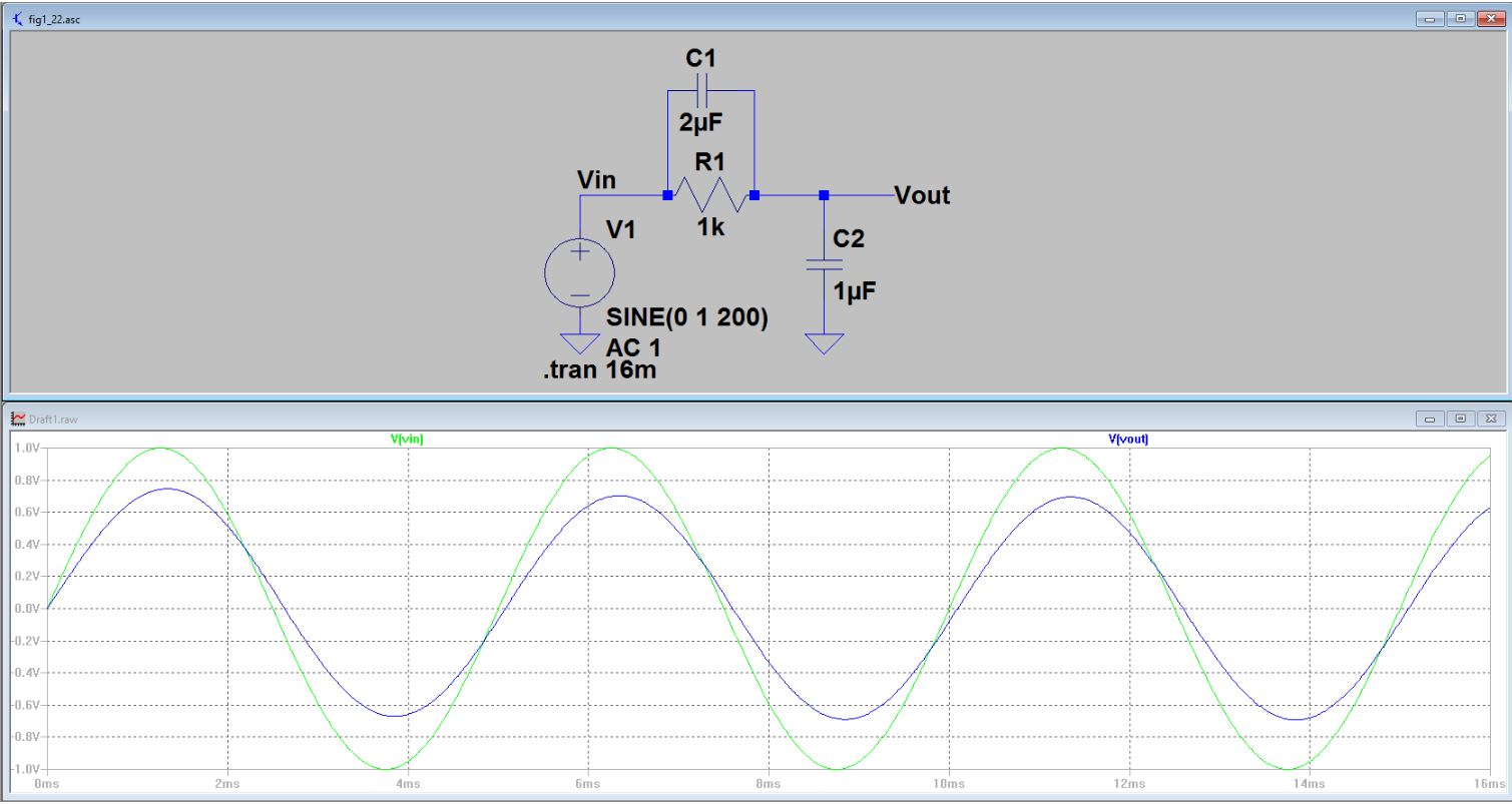
(L) Above is the Transient of Fig1.22 from LTspice
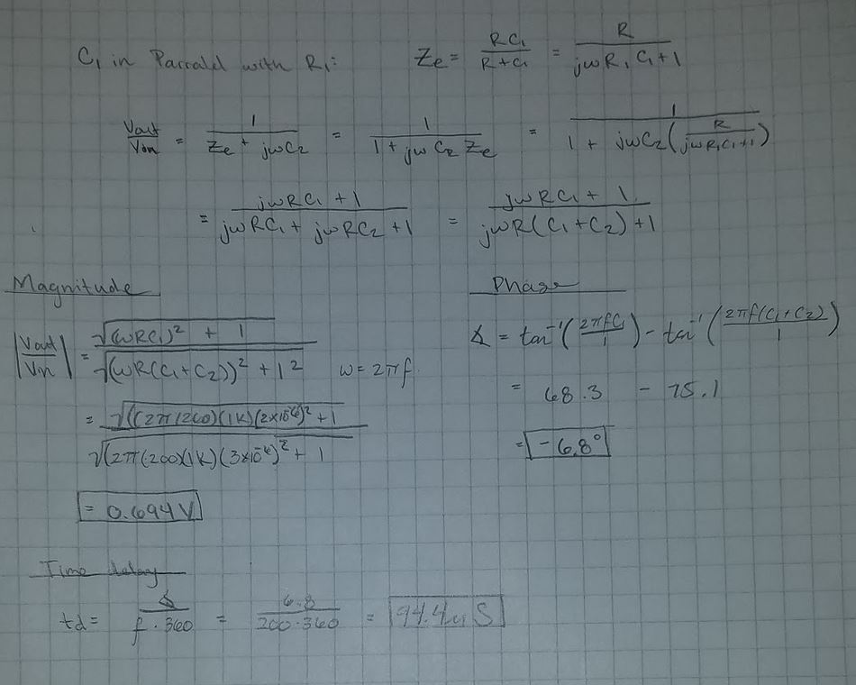
Hand Calculations:
Experimental measurements:
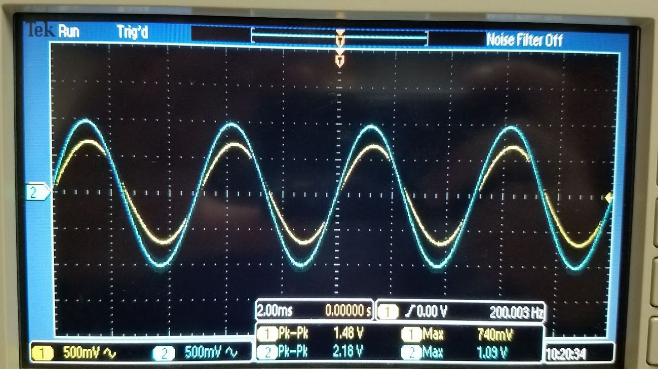
(M)
Magnitude and time delay of experimental circuit. We measure a voltage
of 0.74V at 500mV per square and a delay of approx. 100us. There
exist some error in the automatic measuring or non cursor measurements.
Fig. 1.24
Schematic and Simulation:

(N) Above is the Transient of Fig1.24 from LTspice
Hand Calculations:
Experimental measurements:
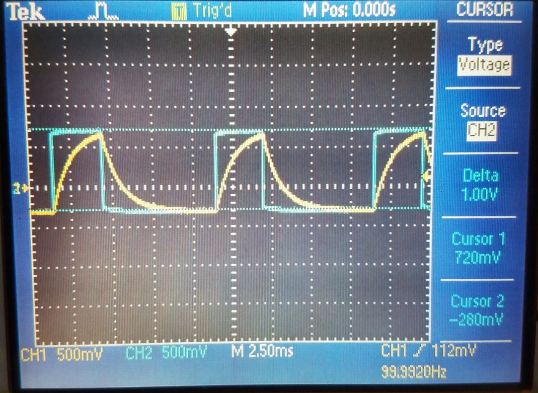
(O) Here we can verify that the peak voltage is 1V
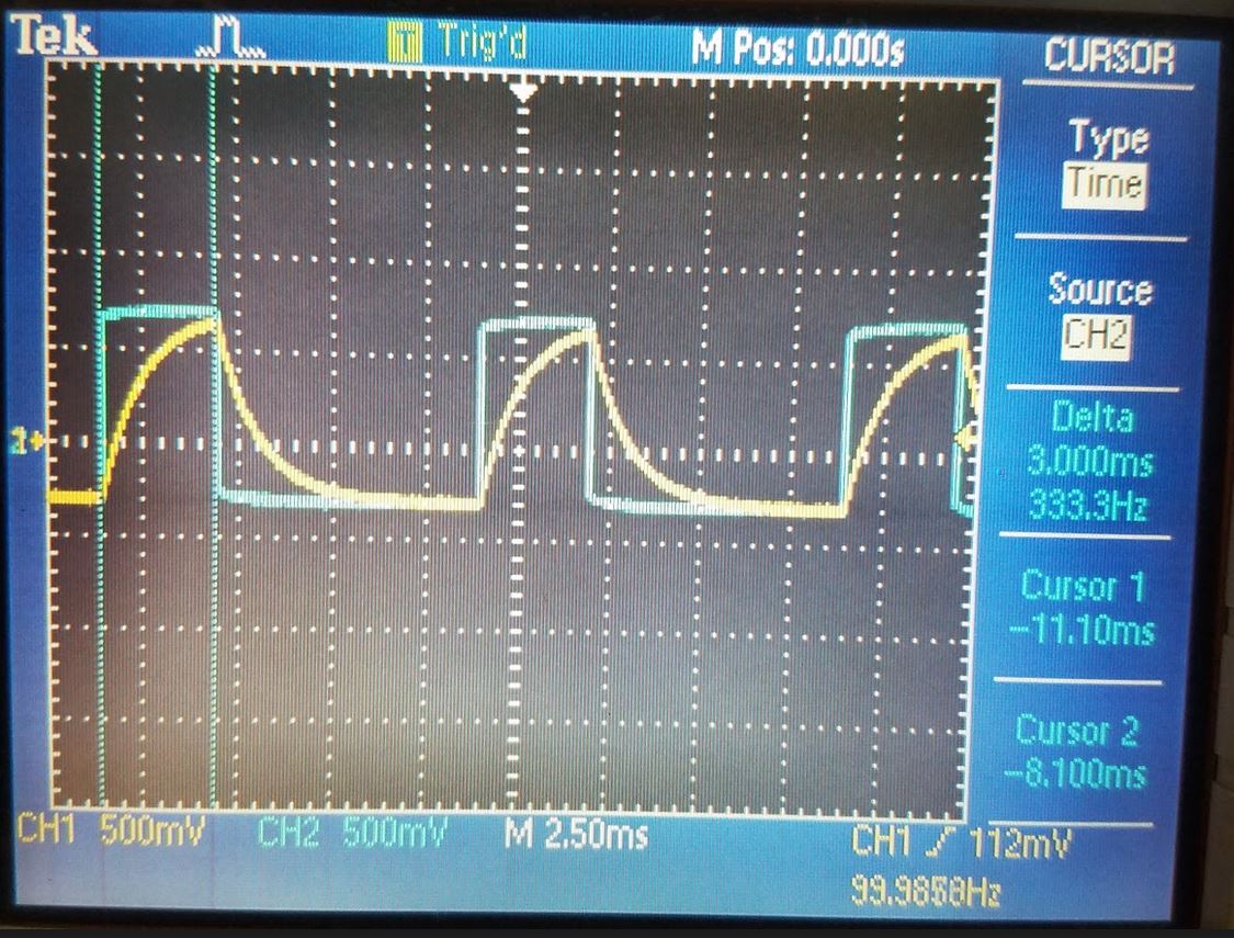
(P)
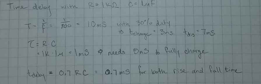
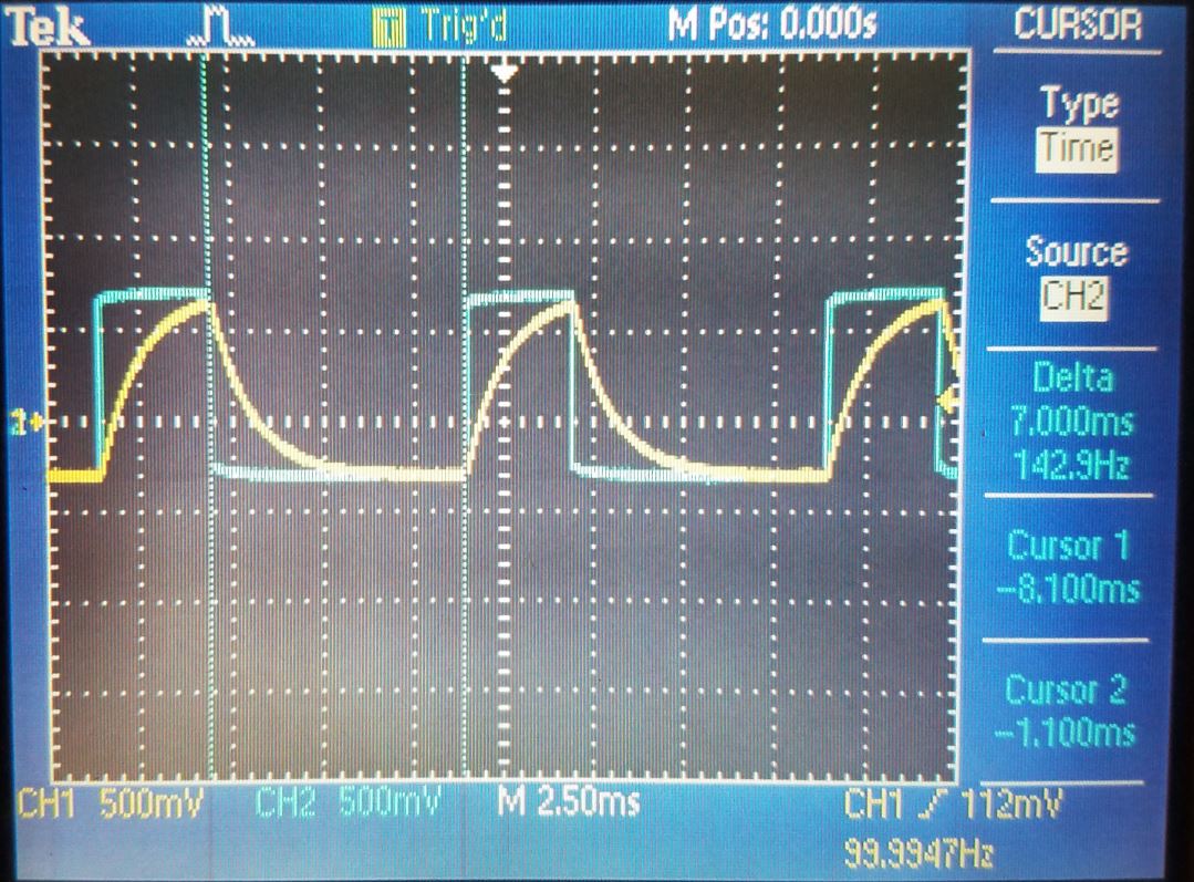
Below we can see the time delay for the rise and fall respectively.
Each vertical line represents 0.5ms, showing a time delay of approx
0.7ms for rise and fall.
Return to butlerk2 EE 420L Reports
Return to EE 420L Labs